Tvs diode arrays, Lightning surge protection - slvu2.8 series, Diodes) – Littelfuse SLVU2.8 Series User Manual
Page 3
© 2013 Littelfuse, Inc.
Specifications are subject to change without notice.
Revised: 04/24/13
TVS Diode Arrays
(SPA
®
Diodes)
Lightning Surge Protection - SLVU2.8 Series
Product Characteristics
Lead Plating
Matte Tin
Lead Material
Copper Alloy
Lead Coplanarity
0.0004 inches (0.102mm)
Substitute Material
Silicon
Body Material
Molded Epoxy
Flammability
UL 94 V-0
Notes :
1. All dimensions are in millimeters
2. Dimensions include solder plating.
3. Dimensions are exclusive of mold flash & metal burr.
4. Blo is facing up for mold and facing down for trim/form, i.e. reverse trim/form.
5. Package surface matte finish VDI 11-13.
Time
Te
mperatur
e
T
P
T
L
T
S(max)
T
S(min)
25
t
P
t
L
t
S
time to peak temperature
Preheat
Preheat
Ramp-up
Ramp-up
Ramp-down
Ramp-do
Critical Zone
T
L
to T
P
Critical Zone
T
L
to T
P
Reflow Condition
Pb – Free assembly
Pre Heat
- Temperature Min (T
s(min)
)
150°C
- Temperature Max (T
s(max)
)
200°C
- Time (min to max) (t
s
)
60 – 180 secs
Average ramp up rate (Liquidus) Temp
(T
L
) to peak
3°C/second max
T
S(max)
to T
L
- Ramp-up Rate
3°C/second max
Reflow
- Temperature (T
L
) (Liquidus)
217°C
- Temperature (t
L
)
60 – 150 seconds
Peak Temperature (T
P
)
260
+0/-5
°C
Time within 5°C of actual peak
Temperature (t
p
)
20 – 40 seconds
Ramp-down Rate
6°C/second max
Time 25°C to peak Temperature (T
P
)
8 minutes Max.
Do not exceed
260°C
Soldering Parameters
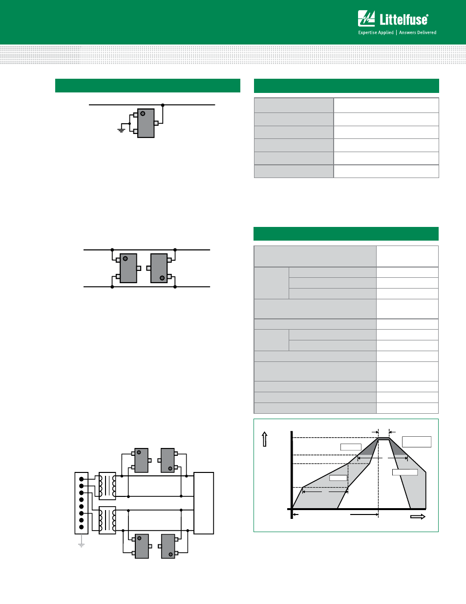
NC
Data Line
Protection of one unidirectional line
Low capacitance protection of one high speed data pair
D1
D2
Ethernet
PHY
J1
J8
RJ-45
Connector
NC
NC
Protection of one unidirectional data line is realized by
connecting pin 3 to the protected line, and pins 1 and 2 to
GND. In this configuration, the device presents a maximum
loading capacitance of tens of picofarads. During positive
transients, the internal TVS diode will conduct and steer
current from pin 3 to 1 (GND), clamping the data line at or
below the specified voltages for the device (see Electrical
Characteristics section). For negative transients, the internal
compensating diode is forward biased, steering the current
from pin 2 (GND) to 3.
Application Example Detail
Low capacitance protection of a high-speed data pair is
realized by connecting two devices in antiparallel. As shown,
pin 1 of the first device is connected to D1 and pin 2 is
connected to D2. Additionally, pin 2 of the second device is
connected to D1 and pin 1 is connected to D2. Pin 3 must be
NC (or not connected) for both devices. When the potential
on D1 exceeds the potential on D2 (by the rated standoff
voltage), pin 2 on the second device will steer current into
pin 1. The compensating diode will conduct in the forward
direction steering current into the avalanching TVS diode
which is operating in the reverse direction. For the opposite
transient, the first device will behave in the same manner. In
this two device arrangement, the total loading capacitance is
two times the rated capacitance from pin 2 to pin 1 which will
typically be much less than 10pF making it suitable for high-
speed data pair such as 10/100/1000 Ethernet.
NC
Data Line
Protection of one unidirectional line
Low capacitance protection of one high speed data pair
D1
D2