Rainbow Electronics MAX111 User Manual
Page 20
MAX110/MAX111
Low-Cost, 2-Channel, ±14-Bit Serial ADCs
20
______________________________________________________________________________________
Capacitive Loading Effects of XCLK in
Internal RC-Oscillator Mode
When using the internal RC oscillator, capacitive load-
ing effects on the XCLK pin must be minimized. Stray
capacitance causes the V
DD
power consumption to
increase by an amount p =
1
⁄
2
CV
2
f, where C = stray
capacitance, V is the supply voltage, and f is the fre-
quency of the internal RC oscillator.
External Reference
The reference inputs to the ADC are high impedance,
allowing both an external voltage reference and ratio-
metric applications without loading effects. The fully dif-
ferential analog signal and reference inputs are
advantageous for performing ratiometric conversions
(Figures 11 and 12). For example, when measuring
load cells, the bridge excitation and the ADC reference
input both share the same voltage source. As the exci-
tation changes with temperature or voltage, the output
of the load cell will change. But since the differential
reference voltage also changes, the conversion results
remain constant, all else remaining equal.
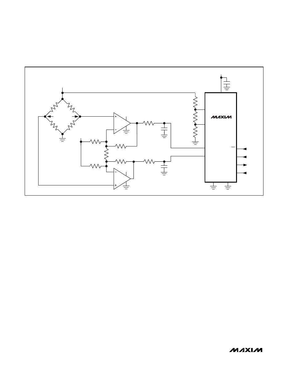
Weigh Scale Application
The fully differential analog signal and reference inputs
make the MAX111 easy to interface to transducers with
differential outputs, such as the load cell in Figure 11.
Because the ADC input is differential, the load cell only
requires differential gain, eliminating the need for the
difference amplifier (differential to single-ended con-
verter) of the standard three op-amp instrumentation-
amplifier realization.
The 30mV full-scale bridge output is amplified to 2V
full-scale and applied to the MAX111 channel-one
input. The reference voltage to the ADC is created by a
voltage divider connected to the +5V rail. The same 5V
provides excitation for the bridge; therefore, as the
excitation voltage varies, the reference voltage to the
ADC also varies, providing an ADC output that does
not depend on the supply voltage.
The two 121k
Ω
resistors connected to the +5V supplies
shift the common-mode voltage from 2.5V (5V/2) to
1.5V to ensure linearity. Match these two resistors to
avoid introducing differential offset, or trim the resistor
mismatch with a potentiometer. In practice, the scale is
“zeroed” or “tared” by storing the average of several
conversions in a memory location while the scale is
+5V
30mV
FULL-SCALE
121k
2k
121k
49.9k
1k
22k
10k
1k
1k
1/2 MAX492
1/2 MAX492
1µF
1µF
REF+
REF-
IN1+
IN1-
AGND
CS
DIN
DOUT
SCLK
49.9k
V
DD
+5V
0.1µF
MAX111
+5V
+5V
+5V
GND
Figure 11. Weigh Scale Application