Rainbow Electronics MAX111 User Manual
Page 17
MAX110/MAX111
Low-Cost, 2-Channel, ±14-Bit Serial ADCs
______________________________________________________________________________________
17
3-Step Calibration
The data sheet electrical specifications apply to the
device after optional calibration of gain error and offset.
Uncalibrated, the gain error is typically 2%.
Table 3 describes the three steps required to calibrate
the ADC completely.
Once the ADC is calibrated to the selected channel, set
CAL = 0 and NUL = 0 and leave CHS unchanged in the
next control word to perform a signal conversion on the
selected analog input channel.
Calibrate the ADC after the following operations:
—
when power is first applied
—
if the reference common-mode voltage changes
—
if the common-mode voltage of the selected input
channel varies significantly. The CMRR of the analog
inputs is 0.25LSB/V.
—
after changing channels (if the common-mode volt-
ages of the two channels are different)
—
after changing conversion speed/resolution.
—
after significant changes in temperature. The offset
drift with temperature is typically 0.003µV/°C.
Automatic gain calibration is not allowed in the
102,400 cycles per conversion mode
(see
Programming Conversion Time
). In this mode, calibra-
tion can be achieved by connecting the reference volt-
age to one input channel and performing a normal
conversion. Subsequent conversion results can be cor-
rected by software.
Do not issue a
N
NO
O--O
OP
P
command
directly following the gain calibration, as the cali-
bration data will be lost.
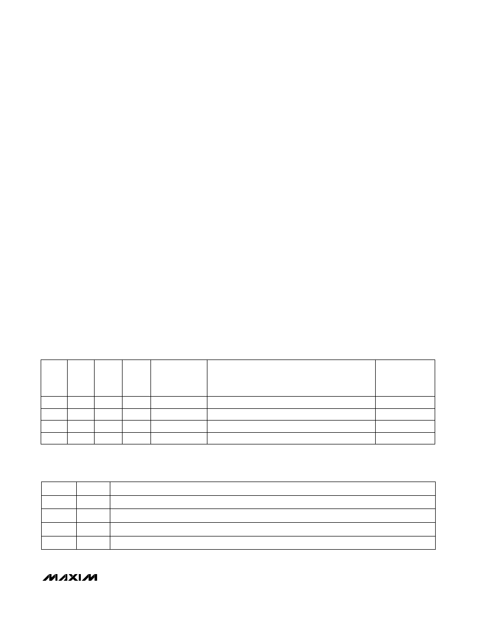
Programming Conversion Time
The MAX110/MAX111 are specified for 12 bits of accu-
racy and up to ±14 bits of resolution. The ADC’s resolu-
tion depends on the number of clock cycles allowed
during each conversion. Control-register bits 9–12
(CONV1–CONV4) determine the conversion time by
controlling the nominal number of oversampling clock
cycles required for each conversion (OSCC/CONV).
Table 4 lists the available conversion times and result-
ing resolutions.
To program a new conversion time, perform a 3-step
calibration with the appropriate CONV1–CONV4 data
used in Table 3. The ADC is now calibrated at the new
conversion speed/resolution.
Table 4. Available Conversion Times
* Gain-calibration mode is not available with 102,400 clock cycles/conversion selected.
Clock duty cycles of 50% ±10% are recommended.
Table 5. Clock Divider-Ratio Control
CONV4 CONV3 CONV2 CONV1
CLOCK CYCLES
PER
CONVERSION
NOMINAL CONVERSION TIME
RCSEL = GND, DV2 = DV4 = 0, XCLK = 500kHz
(ms)
CONVERSION
RESOLUTION
(Bits)
1
0
0
1
10,240
20.48
12 + POL
0
0
1
1
20,480
40.96
13 + POL
0
1
1
0
81,920
163.84
14 + POL
0
0
0
0
102,400*
204.80
14 + POL
Not allowed
1
1
XCLK or internal RC oscillator is divided by 2 and connects to the ADC; f
OSC
= f
XCLK
÷
2.
0
1
XCLK or internal RC oscillator is divided by 4 and connects to the ADC; f
OSC
= f
XCLK
÷
4.
1
0
XCLK or internal RC oscillator connects directly to the ADC; f
OSC
= f
XCLK
.
0
0
DESCRIPTION
DV4
DV2