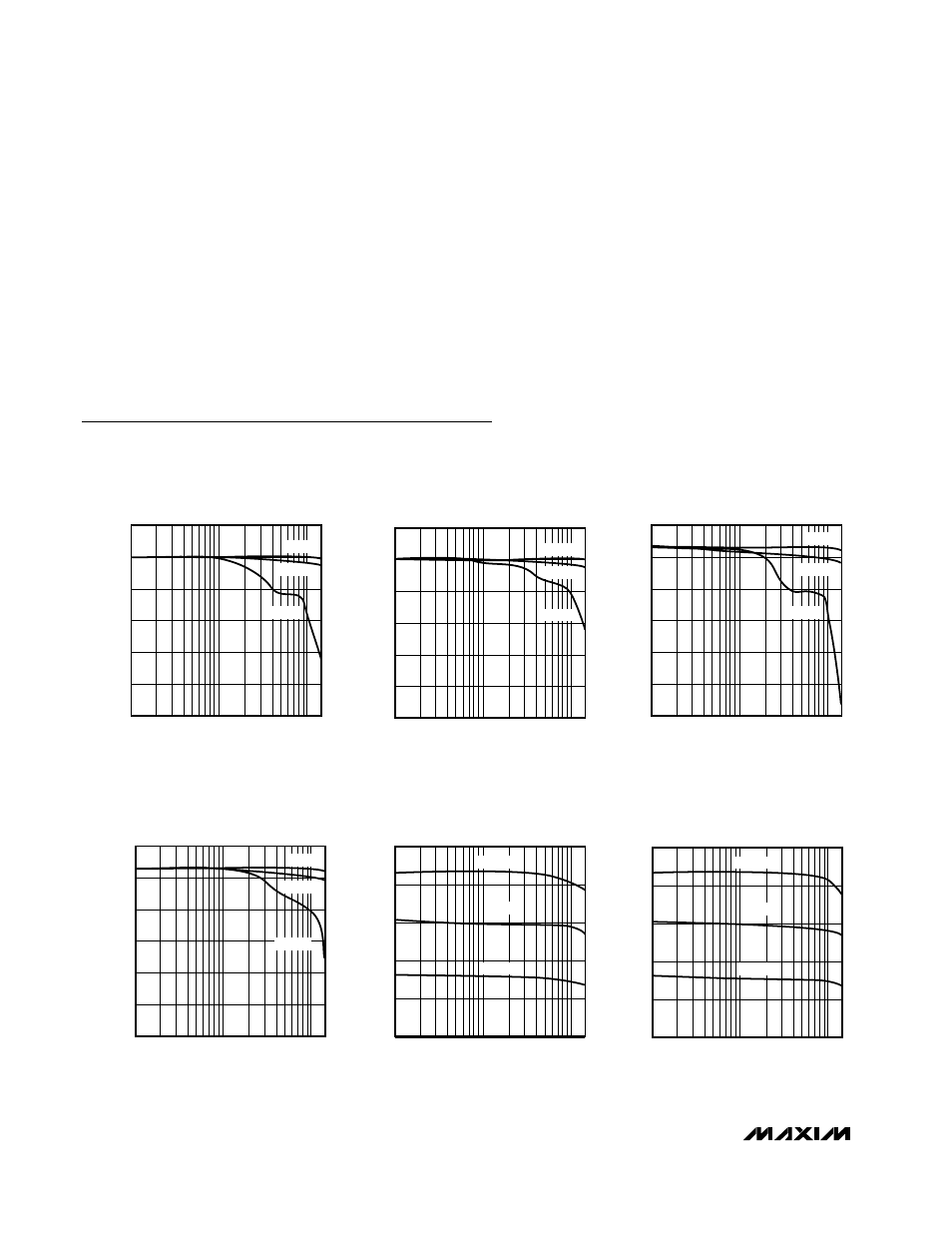
Typical operating characteristics – Rainbow Electronics MAX104 User Manual
Page 6
MAX104
±5V, 1Gsps, 8-Bit ADC with
On-Chip 2.2GHz Track/Hold Amplifier
6
_______________________________________________________________________________________
Typical Operating Characteristics
(V
CC
A = V
CC
I = V
CC
D = +5V, V
EE
= -5V, V
CC
O = +3.3V, REFIN connected to REFOUT, f
S
= 1Gsps, T
A
= +25°C, unless otherwise
noted.)
8.00
6.50
10
100
1000
EFFECTIVE NUMBER OF BITS vs.
ANALOG INPUT FREQUENCY
(SINGLE-ENDED ANALOG INPUT DRIVE)
6.75
7.00
7.25
7.50
7.75
MAX104toc01
ANALOG INPUT FREQUENCY (MHz)
ENOB (Bits)
-12dBFS
-6dBFS
-1dBFS
1250
8.00
6.50
10
100
1000
EFFECTIVE NUMBER OF BITS vs.
ANALOG INPUT FREQUENCY
(DIFFERENTIAL ANALOG INPUT DRIVE)
6.75
7.00
7.25
7.50
7.75
MAX104toc02
ANALOG INPUT FREQUENCY (MHz)
ENOB (Bits)
-12dBFS
-6dBFS
-1dBFS
1250
49
43
10
100
1000
SIGNAL-TO-NOISE PLUS DISTORTION vs.
ANALOG INPUT FREQUENCY
(DIFFERENTIAL ANALOG INPUT DRIVE)
44
45
46
48
47
MAX104toc04
ANALOG INPUT FREQUENCY (MHz)
SINAD (dB)
-12dBFS
-6dBFS
-1dBFS
1250
49
43
10
100
1000
SIGNAL-TO-NOISE PLUS DISTORTION vs.
ANALOG INPUT FREQUENCY
(SINGLE-ENDED ANALOG INPUT DRIVE)
44
45
46
47
48
MAX104toc03
ANALOG INPUT FREQUENCY (MHz)
SINAD (dB)
-12dBFS
-6dBFS
-1dBFS
1250
50
30
10
100
1000
SIGNAL-TO-NOISE RATIO vs.
ANALOG INPUT FREQUENCY
(SINGLE-ENDED ANALOG INPUT DRIVE)
34
38
46
42
MAX104toc05
ANALOG INPUT FREQUENCY (MHz)
SNR (dB)
-12dBFS
-6dBFS
-1dBFS
1250
50
30
10
100
1000 1250
SIGNAL-TO-NOISE RATIO vs.
ANALOG INPUT FREQUENCY
(DIFFERENTIAL ANALOG INPUT DRIVE)
34
38
46
42
MAX104toc06
ANALOG INPUT FREQUENCY (MHz)
SNR (dB)
-12dBFS
-6dBFS
-1dBFS
Note 11:
Effective Number of Bits (ENOB) and Signal-to-Noise Plus Distortion (SINAD) are computed from a curve fit referenced to
the theoretical full-scale range.
Note 12:
Total Harmonic Distortion (THD) is computed from the first five harmonics.
Note 13:
Guaranteed by design with a reset pulse one clock period long or greater.
Note 14:
The DREADY to DATA propagation delay is measured from the 50% point on the rising edge of the DREADY signal (when
the output data changes) to the 50% point on a data output bit. This places the falling edge of the DREADY signal in the
middle of the data output valid window, within the differences between the DREADY and DATA rise and fall times, which
gives maximum setup and hold time for latching external data latches.