Max104, Table 5. dc-coupled clock drive options – Rainbow Electronics MAX104 User Manual
Page 20
MAX104
inputs are AC-coupled. Under this condition, connect
CLKCOM to GNDI. Single-ended ECL/PECL/sine-wave
drive is also possible if the undriven clock input is
reverse-terminated to GNDI through a 50
Ω
resistor in
series with a capacitor whose value is identical to that
used to couple the driven input.
Demux Reset Operation
The MAX104 features an internal 1:2 demultiplexer that
reduces the data rate of the output digital data to one-
half the sample clock rate. Demux reset is necessary
when interleaving multiple MAX104s and/or synchroniz-
ing external demultiplexers. The simplified block diagram
of Figure 1 shows that the demux reset signal path con-
sists of four main circuit blocks. From input to output,
they are the reset input dual latch, the reset pipeline, the
demux clock generator, and the reset output. The sig-
nals associated with the demux reset operation and the
control of this section are listed in Table 6.
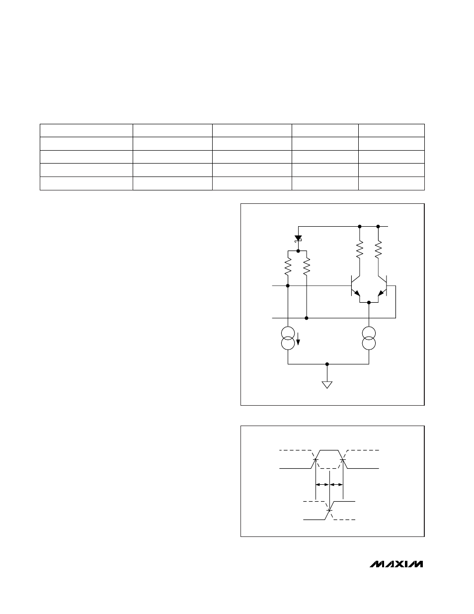
Reset Input Dual Latch
The reset input dual-latch circuit block accepts differ-
ential PECL reset inputs referenced to the same V
CC
O
power supply that powers the MAX104 PECL outputs.
For applications that do not require a synchronizing
reset, the reset inputs can be left open. In this case,
they will self-bias to a proper level with internal 50k
Ω
resistors and 20µA current source. This combination
creates a -1V difference between RSTIN+ and RSTIN-
to disable the internal reset circuitry. When driven with
PECL logic levels terminated with 50
Ω
to (V
CC
O - 2V),
the internal biasing network can easily be overdriven.
Figure 14 shows a simplified schematic of the reset
input structure.
To properly latch the reset input data, the setup time
(t
SU
) and the data hold time (t
HD
) must be met with
respect to the rising edge of the sample clock. The tim-
ing diagram of Figure 15 shows the timing relationship
of the reset input and sampling clock.
±5V, 1Gsps, 8-Bit ADC with
On-Chip 2.2GHz Track/Hold Amplifier
20
______________________________________________________________________________________
Table 5. DC-Coupled Clock Drive Options
-10dBm to +4dBm
Figure 13a
Single-Ended Sine Wave
CLK+
GNDI
CLKCOM
CLOCK DRIVE
REFERENCE
External 50
Ω
to GNDI
CLK-
-10dBm to +4dBm
-10dBm to +4dBm
Figure 13b
Differential Sine Wave
GNDI
ECL Drive
-1.3V
Figure 13c
Single-Ended ECL
-2V
ECL Drive
ECL Drive
Figure 13d
Differential ECL
-2V
50k
50k
RSTIN+
RSTIN-
RESET INPUTS ARE
ESD PROTECTED
(NOT SHOWN IN THIS
SIMPLIFIED DRAWING).
20
µ
A
GNDD
V
CC
O
Figure 14. Simplified Reset Input Structure
RSTIN+
50%
50%
CLK+
CLK-
RSTIN-
50%
t
SU
t
HD
Figure 15. Reset Input Timing Definitions