Detailed description – Rainbow Electronics MAX104 User Manual
Page 12
MAX104
±5V, 1Gsps, 8-Bit ADC with
On-Chip 2.2GHz Track/Hold Amplifier
12
______________________________________________________________________________________
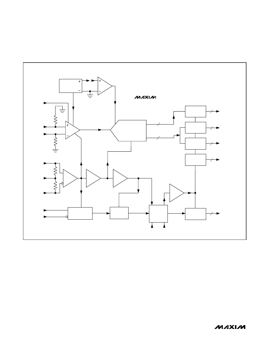
_______________Detailed Description
The MAX104 is an 8-bit, 1Gsps flash analog-to-digital
converter (ADC) with on-chip track/hold (T/H) amplifier
and differential PECL-compatible outputs. The ADC
(Figure 1) employs a fully differential 8-bit quantizer
and a unique encoding scheme to limit metastable
states to typically one error per 10
16
clock cycles, with
no error exceeding 1LSB max.
An integrated 8:16 output demultiplexer simplifies inter-
facing to the part by reducing the output data rate to
one-half the sampling clock rate. This demultiplexer
has internal reset capability that allows multiple
MAX104s to be time-interleaved to achieve higher
effective sampling rates.
When clocked at 1Gsps, the MAX104 provides a typi-
cal effective number of bits (ENOB) of >7.5 bits at an
analog input frequency of 500MHz. The analog input of
the MAX104 is designed for differential or single-ended
use with a ±250mV full-scale input range. In addition,
this ADC features an on-chip +2.5V precision bandgap
reference. If desired, an external reference can also be
used.
CLK-
RSTIN+
RSTIN-
VOSADJ
BANDGAP
REFERENCE
+2.5V
CLK+
CLKCOM
VIN-
VIN+
REF
OUT
REF
IN
DEMUXEN DIVSELECT
DEMUX
CLOCK
DRIVER
16
50
Ω
50
Ω
50
Ω
50
Ω
RSTOUT
A0–A7
P0–P7
DREADY
OR
DIFFERENTIAL
PECL OUTPUTS
T/H
CLOCK
DRIVER
ADC
CLOCK
DRIVER
REFERENCE
AMPLIFIER
2
2
DEMUX
CLOCK
GENERATOR
RESET INPUT
DUAL LATCH
RESET
PIPELINE
GNDI
GNDI
GNDR
DELAYED
RESET
16
16
2
2
T/H AMPLIFIER
LOGIC
CLOCK
DRIVER
BIAS CURRENTS
OVERRANGE
BIT
AUXILIARY
DATA PORT
PRIMARY
DATA PORT
DATA
READY CLOCK
DEMUX
RESET OUTPUT
8-BIT
FLASH ADC
MAX104
Figure 1. Simplified Functional Diagram