Rainbow Electronics MAX104 User Manual
Page 2
MAX104
±5V, 1Gsps, 8-Bit ADC with
On-Chip 2.2GHz Track/Hold Amplifier
2
_______________________________________________________________________________________
ABSOLUTE MAXIMUM RATINGS
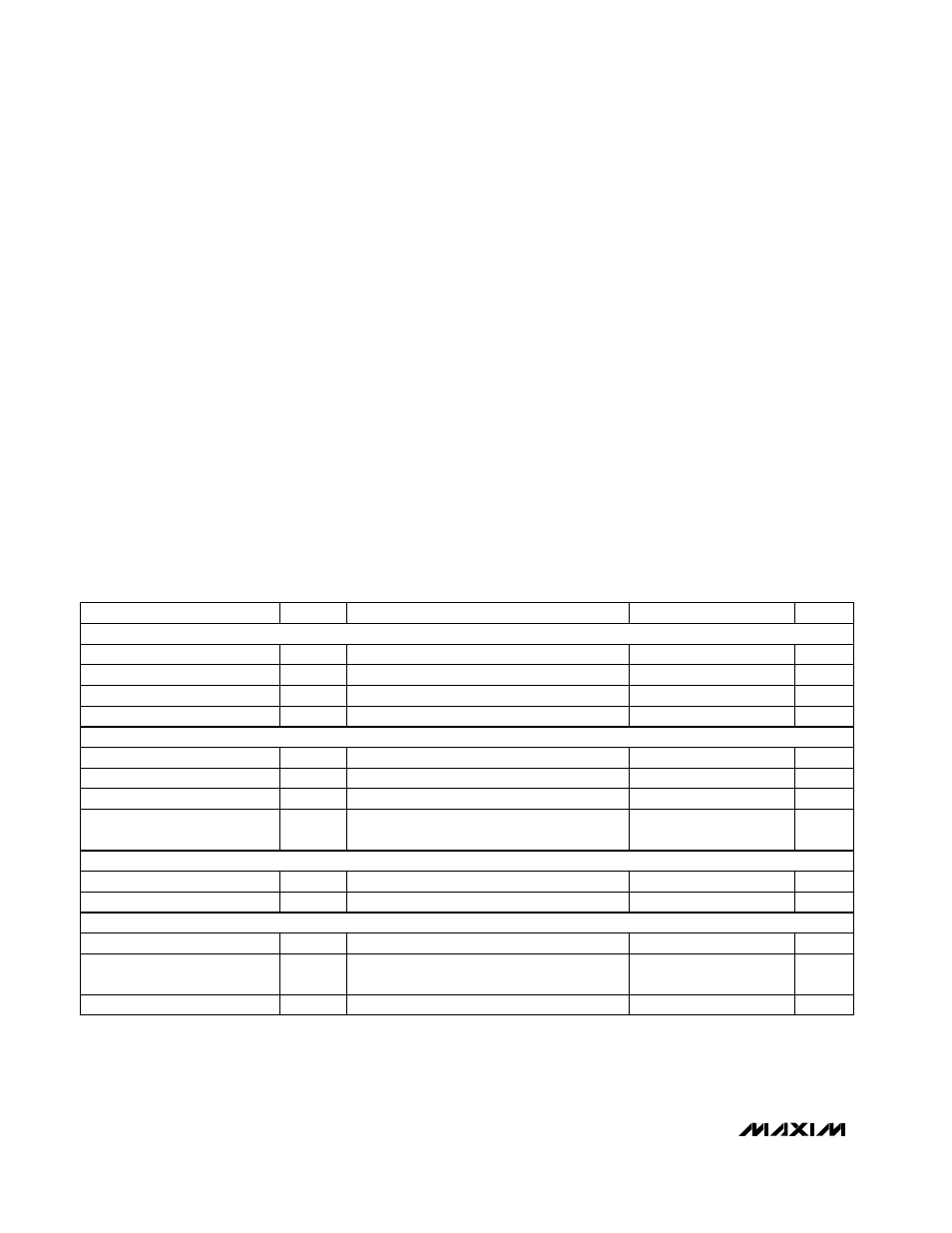
DC ELECTRICAL CHARACTERISTICS
(V
CC
A = V
CC
I = V
CC
D = +5.0V ±5%, V
EE
= -5.0V ±5%, V
CC
O = +3.0V to V
CC
D, REFIN connected to REFOUT, T
A
= T
MIN
to T
MAX
,
unless otherwise noted. Typical values are at T
A
= +25°C.)
Stresses beyond those listed under “Absolute Maximum Ratings” may cause permanent damage to the device. These are stress ratings only, and functional
operation of the device at these or any other conditions beyond those indicated in the operational sections of the specifications is not implied. Exposure to
absolute maximum rating conditions for extended periods may affect device reliability.
V
CC
A to GNDA .........................................................-0.3V to +6V
V
CC
D to GNDD.........................................................-0.3V to +6V
V
CC
I to GNDI ............................................................-0.3V to +6V
V
CC
O to GNDD ........................................-0.3V to (V
CC
D + 0.3V)
AUXEN1, AUXEN2 to GND .....................-0.3V to (V
CC
D + 0.3V)
V
EE
to GNDI..............................................................-6V to +0.3V
Between GNDs......................................................-0.3V to +0.3V
V
CC
A to V
CC
D .......................................................-0.3V to +0.3V
V
CC
A to V
CC
I .........................................................-0.3V to +0.3V
PECL Digital Output Current ...............................................50mA
REFIN to GNDR ........................................-0.3V to (V
CC
I + 0.3V)
REFOUT Current ................................................+100µA to -5mA
ICONST, IPTAT to GNDI .......................................-0.3V to +1.0V
TTL/CMOS Control Inputs (DEMUXEN,
DIVSELECT)..........................................-0.3V to (V
CC
D + 0.3V)
RSTIN+, RSTIN- ......................................-0.3V to (V
CC
O + 0.3V)
VOSADJ Adjust Input ................................-0.3V to (V
CC
I + 0.3V)
CLK+ to CLK- Voltage Difference..........................................±3V
CLK+, CLK-.....................................(V
EE
- 0.3V) to (GNDD + 1V)
CLKCOM.........................................(V
EE
- 0.3V) to (GNDD + 1V)
VIN+ to VIN- Voltage Difference ............................................±2V
VIN+, VIN- to GNDI................................................................±2V
Continuous Power Dissipation (T
A
= +70°C)
192-Contact ESBGA (derate 61mW/°C above +70°C) ......4.88W
(with heatsink and 200 LFM airflow,
derate 106mW/°C above +70°C) ........................................8.48W
Operating Temperature Range
MAX104CHC........................................................0°C to +70°C
Operating Junction Temperature.....................................+150°C
Storage Temperature Range .............................-65°C to +150°C
T
A
= +25°C
Referenced to GNDR
0 < I
SOURCE
< 2.5mA
Driving REFIN input only
VIN+ and VIN- to GNDI, T
A
= +25°C
VOSADJ = 0 to 2.5V
Signal + offset w.r.t. GNDI
Note 1
T
A
= +25°C
No missing codes guaranteed
CONDITIONS
k
Ω
4
5
R
REF
Reference Input Resistance
mV
5
∆
REFOUT
Reference Output Load
Regulation
V
2.475
2.50
2.525
REFOUT
Reference Output Voltage
LSB
±4
±5.5
Input V
OS
Adjust Range
k
Ω
14
25
R
VOS
Input Resistance (Note 2)
LSB
-0.5
±0.25
0.5
INL
Integral Nonlinearity (Note 1)
Bits
8
RES
Resolution
ppm/°C
150
TC
R
Input Resistance Temperature
Coefficient
Ω
49
50
51
R
IN
Input Resistance
V
±0.8
V
CM
Common-Mode Input Range
mVp-p
475
500
525
V
FSR
Full-Scale Input Range
LSB
-0.5
±0.25
0.5
DNL
Differential Nonlinearity (Note 1)
Codes
None
Missing Codes
UNITS
MIN
TYP
MAX
SYMBOL
PARAMETER
ACCURACY
ANALOG INPUTS
VOS ADJUST CONTROL INPUT
REFERENCE INPUT AND OUTPUT