Principle of operation, On-chip track/hold amplifier, Internal reference – Rainbow Electronics MAX104 User Manual
Page 13
Principle of Operation
The MAX104’s flash or parallel architecture provides
the fastest multibit conversion of all common integrated
ADC designs. The key to this high-speed flash archi-
tecture is the use of an innovative, high-performance
comparator design. The flash converter and down-
stream logic translate the comparator outputs into a
parallel 8-bit output code and pass this binary code on
to the optional 8:16 demultiplexer, where primary and
auxiliary ports output PECL-compatible data at up to
500Msps per port (depending on how the demultiplex-
er section is set on the MAX104).
The ideal transfer function appears in Figure 2.
On-Chip Track/Hold Amplifier
As with all ADCs, if the input waveform is changing
rapidly during conversion, effective number of bits
(ENOB) and signal-to-noise ratio (SNR) specifications
will degrade. The MAX104’s on-chip, wide-bandwidth
(2.2GHz) T/H amplifier reduces this effect and increases
the ENOB performance significantly, allowing precise
capture of fast analog data at high conversion rates.
The T/H amplifier buffers the input signal and allows a
full-scale signal input range of ±250mV. The T/H ampli-
fier’s differential 50
Ω
input termination simplifies inter-
facing to the MAX104 with controlled impedance lines.
Figure 3 shows a simplified diagram of the T/H amplifier
stage internal to the MAX104.
Aperture width, delay, and jitter (or uncertainty) are
parameters that affect the dynamic performance of
high-speed converters. Aperture jitter, in particular,
directly influences SNR and limits the maximum slew
rate (dV/dt) that can be digitized without contributing
significant errors. The MAX104’s innovative T/H amplifier
design limits aperture jitter typically to less than 0.5ps.
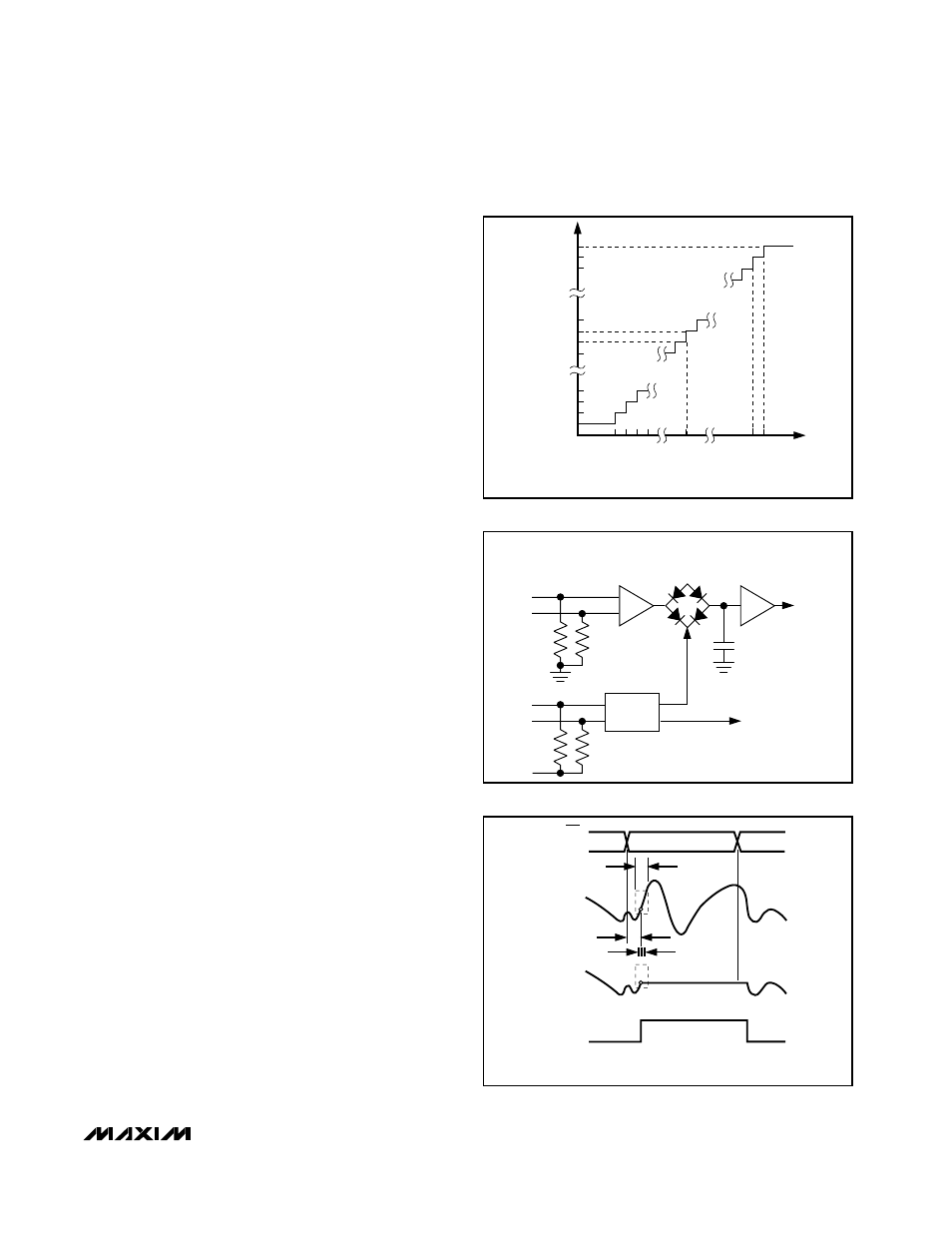
Aperture Width
Aperture width (t
AW
) is the time the T/H circuit requires
(Figure 4) to disconnect the hold capacitor from the
input circuit (for instance, to turn off the sampling
bridge and put the T/H unit in hold mode).
Aperture Jitter
Aperture jitter (t
AJ
) is the sample-to-sample variation
(Figure 4) in the time between the samples.
Aperture Delay
Aperture delay (t
AD
) is the time defined between the
rising edge of the sampling clock and the instant when
an actual sample is taken (Figure 4).
Internal Reference
The MAX104 features an on-chip +2.5V precision
bandgap reference, which can be used by connecting
MAX104
±5V, 1Gsps, 8-Bit ADC with
On-Chip 2.2GHz Track/Hold Amplifier
______________________________________________________________________________________
13
(-FS + 1LSB)
0
+FS
(+FS - 1LSB)
255
255
254
129
128
127
126
3
2
1
0
ANALOG INPUT
OVERRANGE +
DIGITAL OUTPUT
Figure 2. Transfer Function
HOLD
CLK
ANALOG
INPUT
SAMPLED
DATA (T/H)
T/H
t
AW
t
AD
t
AJ
TRACK
TRACK
APERTURE DELAY (t
AD
)
APERTURE WIDTH (t
AW
)
APERTURE JITTER (t
AJ
)
CLK
Figure 4. T/H Aperture Timing
TO
COMPARATORS
TO
COMPARATORS
BUFFER
AMPLIFIER
INPUT
AMPLIFIER
CLOCK
SPLITTER
ALL INPUTS ARE ESD PROTECTED
(NOT SHOWN IN THIS
SIMPLIFIED DRAWING).
SAMPLING
BRIDGE
GNDI
50
Ω
50
Ω
VIN+
VIN-
GNDI
C
HOLD
50
Ω
50
Ω
CLK+
CLK-
CLKCOM
Figure 3. Internal Structure of the 2.2GHz T/H Amplifier