Max104 – Rainbow Electronics MAX104 User Manual
Page 18
MAX104
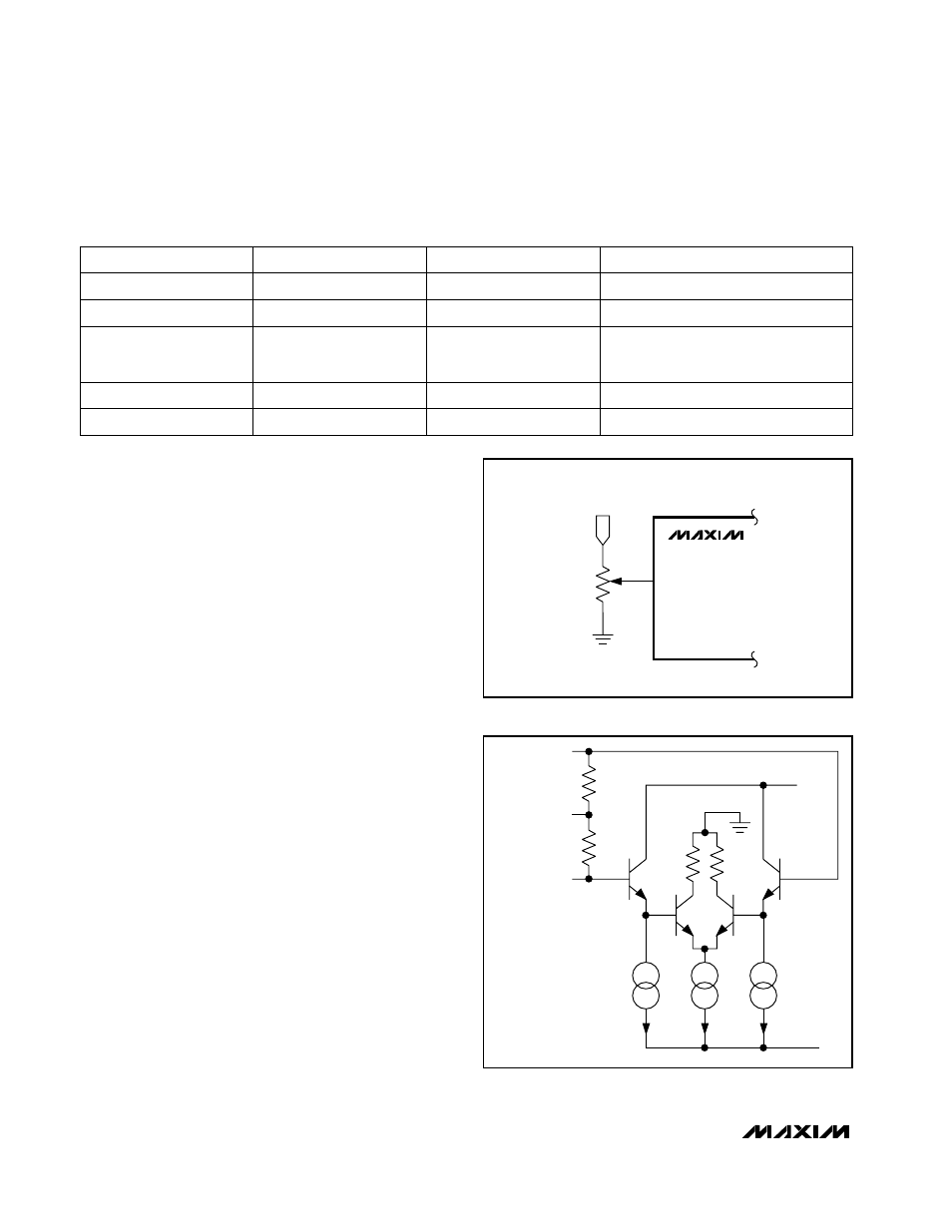
Offset Adjust
The MAX104 provides a control input (VOSADJ) to com-
pensate for system offsets. The offset adjust input is a
self-biased voltage divider from the internal +2.5V preci-
sion reference. The nominal open-circuit voltage is one-
half the reference voltage. With an input resistance of
typically 25k
Ω
, this pin may be driven by an external
10k
Ω
potentiometer (Figure 11) connected between
REFOUT and GNDI to correct for offset errors. This con-
trol provides a typical ±5.5LSB offset adjustment range.
Clock Operation
The MAX104 clock inputs are designed for either single-
ended or differential operation (Figure 12) with flexible
input drive requirements. Each clock input is terminated
with an on-chip, laser-trimmed 50
Ω
resistor to CLKCOM
(clock-termination return). The CLKCOM termination
voltage can be connected anywhere between ground
and -2V for compatibility with standard ECL drive levels.
The clock inputs are internally buffered with a preampli-
fier to ensure proper operation of the data converter
with even small-amplitude sine-wave sources. The
MAX104 was designed for single-ended, low-phase-
noise sine-wave clock signals with as little as 100mV
amplitude (-10dBm). This eliminates the need for an
external ECL clock buffer and its added jitter.
Single-Ended Clock Inputs (Sine-Wave Drive)
Excellent performance is obtained by AC- or DC-cou-
pling a low-phase-noise sine-wave source into a single
clock input (Figure 13a, Table 5). For proper DC bal-
ance, the undriven clock input should be externally
50
Ω
reverse-terminated to GNDI.
The dynamic performance of the data converter is
essentially unaffected by clock-drive power levels from
±5V, 1Gsps, 8-Bit ADC with
On-Chip 2.2GHz Track/Hold Amplifier
18
______________________________________________________________________________________
Table 4. Ideal Input Voltage and Output Code Results for Differential Operation
-125mV
-125mV + 0.5LSB
11111111 (full scale)
+125mV
VIN-
1
11111111
+125mV - 0.5LSB
0
OVERRANGE BIT
0V
+125mV - 0.5LSB
01111111
toggles
10000000
0V
0
00000001
-125mV + 0.5LSB
0
+125mV
00000000 (zero scale)
-125mV
0
VIN+
OUTPUT CODE
GNDI
POT
10k
REFOUT
VOSADJ
MAX104
Figure 11. Offset Adjust with External 10k
Ω
Potentiometer
CLK+
CLKCOM
CLOCK INPUTS ARE
ESD PROTECTED
(NOT SHOWN IN THIS
SIMPLIFIED DRAWING).
CLK-
50
Ω
+0.8V
50
Ω
GNDI
V
EE
Figure 12. Simplified Clock Input Structure (Single-Ended/
Differential)