0 lm63 registers – Rainbow Electronics LM63 User Manual
Page 15
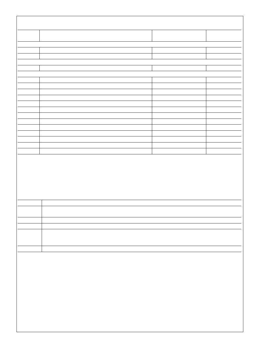
2.0 LM63 Registers
(Continued)
Register
[HEX]
Register Name
Read/Write
POR Default
[HEX]
ALERT STATUS AND MASK REGISTERS
02
ALERT Status
Read Only
N/A
16
ALERT Mask
R/W
A4
ID AND TEST REGISTERS
FF
Stepping/Die Rev. ID
Read Only
41
[RESERVED] REGISTERS — NOT USED
06
Not Used
N/A
N/A
0C
Not Used
N/A
N/A
15
Not Used
N/A
N/A
17
Not Used
N/A
N/A
18
Not Used
N/A
N/A
1A–1F
Not Used
N/A
N/A
20
Not Used
N/A
N/A
22–2F
Not Used
N/A
N/A
30–3F
Not Used
N/A
N/A
40–45
Not Used
N/A
N/A
4E
Not Used
N/A
N/A
60–BE
Not Used
N/A
N/A
C0–FD
Not Used
N/A
N/A
2.3 LM63 INITIAL REGISTER SEQUENCE AND REGISTER DESCRIPTIONS IN FUNCTIONAL ORDER
The following is a Register Map grouped in functional and sequence order. Some address locations have been left blank to
maintain compatibility with LM86. Addresses in parenthesis are mirrors of named address for backwards compatibility with some
older software. Reading or writing either address will access the same 8-bit register.
2.3.1 LM63 Required Initial Fan Control Register Sequence
Important! The BIOS must follow the sequence below to configure the following Fan Registers for the LM63 before using any of
the Fan or Tachometer or PWM registers:
Step
[Register]
HEX
and Setup Instructions
1
[4A] Write bits 0 and 1; 3 and 4. This includes tach settings if used, PWM internal clock select (1.4 kHz or
360 kHz) and PWM Output Polarity.
2
[4B] Write bits 0 through 5 to program the spin-up settings.
3
[4D] Write bits 0 through 4 to set the frequency settings. This works with the PWM internal clock select.
4
Choose, then write, only one of the following:
A. [4F–5F] the Lookup Table, or
B. [4C] the PWM value bits 0 through 5.
5
If Step 4A, Lookup Table, was chosen and written then write [4A] bit 5 = 0.
All other registers can be written at any time after the above sequence.
LM63
www.national.com
15