Electrical characteristics (continued) – Rainbow Electronics MAX1545 User Manual
Page 8
MAX1519/MAX1545
Dual-Phase, Quick-PWM Controllers for
Programmable CPU Core Power Supplies
8
_______________________________________________________________________________________
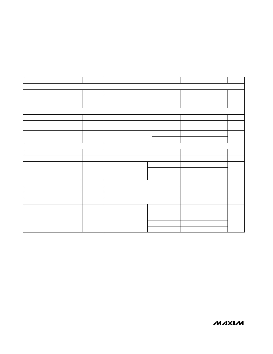
ELECTRICAL CHARACTERISTICS (continued)
(Circuit of Figure 1, V+ = 15V, V
CC
= V
DD
= V
SHDN
= V
TON
= V
SKIP
= V
S0
= V
S1
= V
CODE
= 5V, V
FB
= V
CMP
= V
CMN
= V
CSP
= V
CSN
= 1.3V, OFS = SUS = GNDS = D0–D4 = GND; T
A
= -40°C to +100°C, unless otherwise specified.) (Note 5)
PARAMETER
SYMBOL
CONDITIONS
MIN
TYP
MAX
UNITS
GATE DRIVERS
DH_ Gate-Driver On-Resistance
R
ON(DH)
BST_ - LX_ forced to 5V
4.5
Ω
High state (pullup)
4.5
DL_ Gate-Driver On-Resistance
R
ON(DL)
Low start (pulldown)
2
Ω
VOLTAGE-POSITIONING AMPLIFIER
Input Offset Voltage
V
OS
-2.0
+2.0
mV
Common-Mode Input Voltage
Range
V
CM
Guaranteed by CMRR test
0
2.5
V
V
CC
- V
FBH
300
Output Voltage Swing
|V
OAIN+
- V
OAIN-
|
≥ 10mV,
R
L
= 1k
Ω to V
CC
/2
V
FBL
200
mV
LOGIC AND I/O
SHDN Input High Voltage
V
IH
0.8
V
SHDN Input Low Voltage
V
IL
0.4
V
High
2.7
REF
1.2
2.3
Three-Level Input Logic Levels
SUS,
SKIP
Low
0.8
V
D0–D4 Logic Input High Voltage
1.6
V
D0–D4 Logic Input Low Voltage
0.8
V
CODE Input High Voltage
2.4
V
CODE Input Low Voltage
0.8
V
High
V
CC
-
0.4
Open
3.15
3.85
REF
1.65
2.35
Four-Level Input Logic Levels
TON, S0–S1
Low
0.4
V
Note 2: DC output accuracy specifications refer to the trip level of the error amplifier. When pulse skipping, the output slightly rises
(< 0.5%) when transitioning from continuous conduction to no load.
Note 3: On-time and minimum off-time specifications are measured from 50% to 50% at the DHM and DHS pins, with LX_ forced to
GND, BST_ forced to 5V, and a 500pF capacitor from DH_ to LX_ to simulate external MOSFET gate capacitance. Actual in-
circuit times may be different due to MOSFET switching speeds.
Note 4: The output fault-blanking time is measured from the time when FB reaches the regulation voltage set by the DAC code.
During normal operation (SUS = GND), regulation voltage is set by the VID DAC inputs (D0–D4). During suspend mode
(SUS = REF or high), the regulation voltage is set by the suspend DAC inputs (S0–S1).
Note 5: Specifications to T
A
= -40°C and +100°C are guaranteed by design and are not production tested.