Rainbow Electronics MAX1545 User Manual
Page 35
MAX1519/MAX1545
Dual-Phase, Quick-PWM Controllers for
Programmable CPU Core Power Supplies
______________________________________________________________________________________
35
For the low-side MOSFET (N
L
), the worst-case power
dissipation always occurs at maximum input voltage:
The worst-case for MOSFET power dissipation occurs
under heavy overloads that are greater than
I
LOAD(MAX)
but are not quite high enough to exceed
the current limit and cause the fault latch to trip. To pro-
tect against this possibility, you can “overdesign” the
circuit to tolerate:
where I
VALLEY(MAX)
is the maximum valley current
allowed by the current-limit circuit, including threshold
tolerance and on-resistance variation. The MOSFETs
must have a good size heatsink to handle the overload
power dissipation.
Choose a Schottky diode (D
L
) with a forward voltage
low enough to prevent the low-side MOSFET body
diode from turning on during the dead time. As a gen-
eral rule, select a diode with a DC current rating equal
to 1/3 of the load current-per-phase. This diode is
optional and can be removed if efficiency is not critical.
Boost Capacitors
The boost capacitors (C
BST
) selected must be large
enough to handle the gate-charging requirements of
the high-side MOSFETs. Typically, 0.1µF ceramic
capacitors work well for low-power applications driving
medium-sized MOSFETs. However, high-current appli-
cations driving large, high-side MOSFETs require boost
capacitors larger than 0.1µF. For these applications,
select the boost capacitors to avoid discharging the
capacitor more than 200mV while charging the high-
side MOSFET’s gates:
where N is the number of high-side MOSFETs used for
one regulator, and Q
GATE
is the gate charge specified
in the MOSFET’s data sheet. For example, assume (2)
IRF7811W N-channel MOSFETs are used on the high
side. According to the manufacturer’s data sheet, a sin-
gle IRF7811W has a maximum gate charge of 24nC
(V
GS
= 5V). Using the above equation, the required
boost capacitance would be:
Selecting the closest standard value, this example
requires a 0.22µF ceramic capacitor.
C
x
nC
mV
F
BST
=
=
2
24
200
0 24
.
µ
C
N x Q
mV
BST
GATE
=
200
I
I
I
I
I
LIR
LOAD
TOTA L VALLEY MAX
INDUCTOR
TOTAL VALLEY MAX
LOAD MAX
=
+
=
+
η
η
(
)
(
)
(
)
∆
2
2
PD N RESISTIVE
V
V
I
R
L
OUT
IN MAX
LOAD
TOTAL
DS ON
(
)
(
)
(
)
=
−
1
2
η
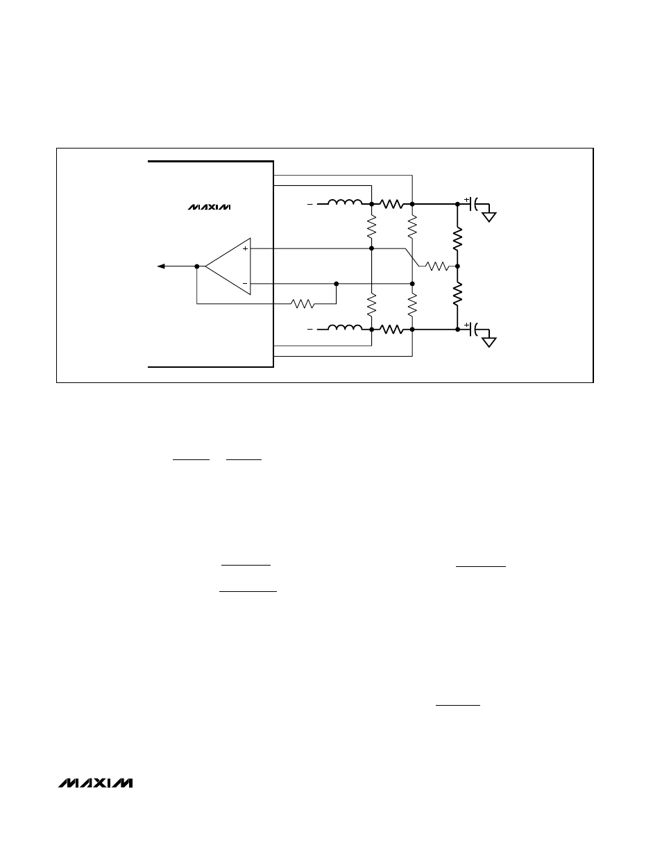
MAIN
PHASE
SECOND
PHASE
PC BOARD TRACE
RESISTANCE
ERROR
COMPARATOR
R
F
R
A
R
A
R
B
R
B
OAIN+
OAIN-
FB
PC BOARD TRACE
RESISTANCE
CPU SENSE
POINT
CMP
CMN
CSP
CSN
L1
R
SENSE
R
FBS
L2
R
SENSE
MAX1519
MAX1545
Figure 10. Voltage-Positioning Gain