Absolute maximum ratings, Electrical characteristics – Rainbow Electronics MAX1545 User Manual
Page 2
MAX1519/MAX1545
Dual-Phase, Quick-PWM Controllers for
Programmable CPU Core Power Supplies
2
_______________________________________________________________________________________
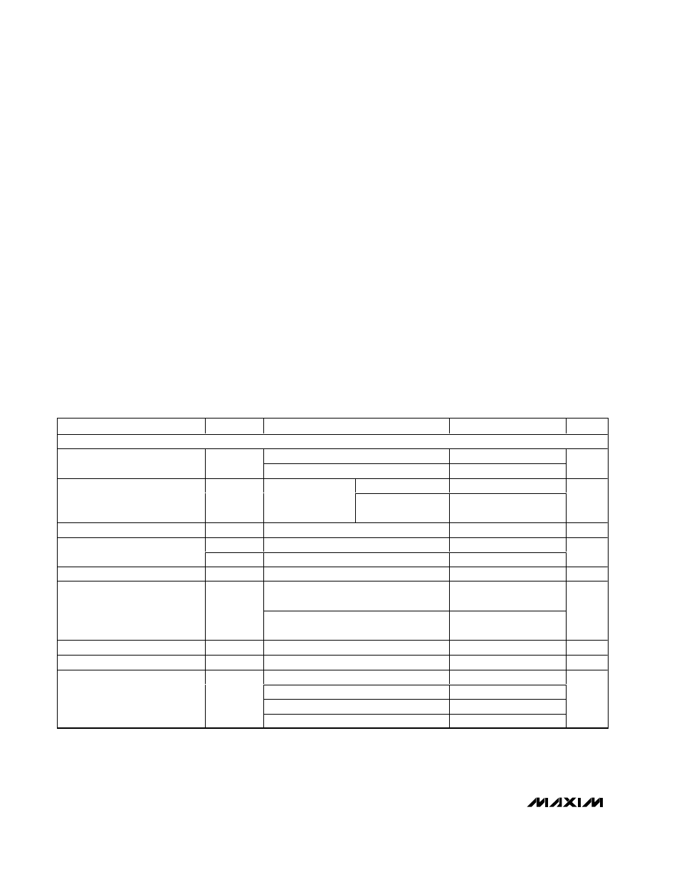
ABSOLUTE MAXIMUM RATINGS
Stresses beyond those listed under “Absolute Maximum Ratings” may cause permanent damage to the device. These are stress ratings only, and functional
operation of the device at these or any other conditions beyond those indicated in the operational sections of the specifications is not implied. Exposure to
absolute maximum rating conditions for extended periods may affect device reliability.
V+ to GND ..............................................................-0.3V to +30V
V
CC
to GND ..............................................................-0.3V to +6V
V
DD
to PGND............................................................-0.3V to +6V
SKIP, SUS, D0–D4 to GND.......................................-0.3V to +6V
ILIM, FB, OFS, CCV, CCI, REF, OAIN+,
OAIN- to GND.........................................-0.3V to (V
CC
+ 0.3V)
CMP, CSP, CMN, CSN, GNDS to GND ......-0.3V to (V
CC
+ 0.3V)
TON, TIME, VROK, S0–S1, CODE to GND.-0.3V to (V
CC
+ 0.3V)
SHDN to GND (Note 1)...........................................-0.3V to +18V
DLM, DLS to PGND ....................................-0.3V to (V
DD
+ 0.3V)
BSTM, BSTS to GND ..............................................-0.3V to +36V
DHM to LXM ...........................................-0.3V to (V
BSTM
+ 0.3V)
LXM to BSTM............................................................-6V to +0.3V
DHS to LXS..............................................-0.3V to (V
BSTS
+ 0.3V)
LXS to BSTS .............................................................-6V to +0.3V
GND to PGND .......................................................-0.3V to +0.3V
REF Short-Circuit Duration .........................................Continuous
Continuous Power Dissipation (T
A
= +70°C)
40-Pin 6mm
✕
6mm Thin QFN
(derate 23.2mW/°C above +70°C) ...............................1.860W
Operating Temperature Range .........................-40°C to +100°C
Junction Temperature ......................................................+150°C
Storage Temperature Range .............................-65°C to +150°C
Lead Temperature (soldering, 10s) .................................+300°C
ELECTRICAL CHARACTERISTICS
(Circuit of Figure 1, V+ = 15V, V
CC
= V
DD
= V
SHDN
= V
TON
= V
SKIP
= V
S0
= V
S1
= V
CODE
= 5V, V
FB
= V
CMP
= V
CMN
= V
CSP
= V
CSN
= 1.3V, OFS = SUS = GNDS = D0–D4 = GND; T
A
= 0°C to +85°C, unless otherwise specified. Typical values are at T
A
= +25°C.)
PARAMETER
SYMBOL
CONDITIONS
MIN
TYP
MAX
UNITS
PWM CONTROLLER
Battery voltage, V+
4
28
Input Voltage Range
V
CC
, V
DD
4.5
5.5
V
DAC codes
≥ 1V
-10
+10
DC Output Voltage Accuracy
(Note 2)
V+ = 4.5V to 28V,
includes load
regulation error
DAC codes from
0.60V to 1V
-15
+15
mV
Line Regulation Error
V
CC
= 4.5V to 5.5V, V+ = 4.5V to 28V
5
mV
I
FB
, I
GNDS
FB, GNDS
-2
+2
Input Bias Current
I
OFS
OFS
-0.1
+0.1
µA
OFS Input Range
0
2
V
∆V
OUT
/
∆V
OFS;
∆V
OFS
= V
OFS,
V
OFS
= 0 to 1V
-0.129
-0.125
-0.117
OFS Gain
A
OFS
∆V
OUT
/
∆V
OFS;
∆V
OFS
= V
OFS
- V
REF,
V
OFS
= 1V to 2V
-0.129
-0.125
-0.117
V/V
GNDS Input Range
-20
+200
mV
GNDS Gain
A
GNDS
∆V
OUT
/
∆V
GNDS
0.97
0.99
1.01
V/V
1000kHz nominal, R
TIME
= 15k
Ω
900
1000
1100
500kHz nominal, R
TIME
= 30k
Ω
460
500
540
250kHz nominal, R
TIME
= 60k
Ω
225
250
275
TIME Frequency Accuracy
f
TIME
Shutdown, R
TIME
= 30k
Ω
125
kHz
Note 1: SHDN may be forced to 12V for the purpose of debugging prototype boards using the no-fault test mode, which disables
fault protection and overlapping operation.