Rainbow Electronics MAX2062 User Manual
Page 4

4 ______________________________________________________________________________________
MAX2062
Dual 50MHz to 1000MHz High-Linearity,
Serial/Parallel-Controlled Analog/Digital VGA
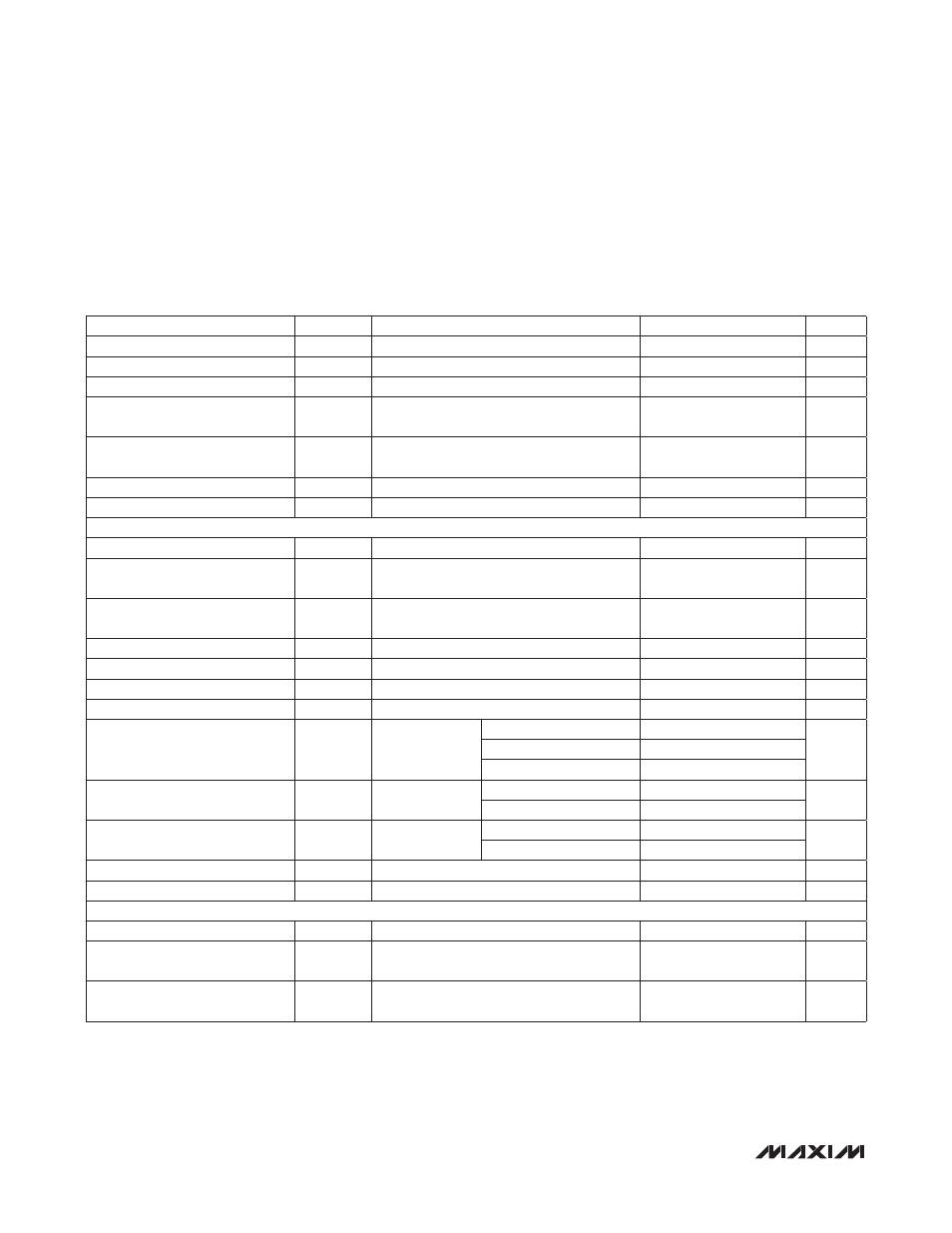
5.0V SUPPLy AC ELECTRICAL CHARACTERISTICS (Each Path, Unless Otherwise
Noted) (continued)
(Typical Application Circuit, V
CC
= V
CC_AMP_1
= V
CC_AMP_2
= V
CC_RG
= 4.75V to 5.25V, attenuators are set for maximum gain, RF
ports are driven from 50I sources, AMPSET = 0, PD_1 = PD_2 = 0, 100MHz P f
RF
P 500MHz, T
C
= -40NC to +85NC. Typical values
are at maximum gain setting, V
CC
= 5.0V, P
IN
= -20dBm, f
RF
= 350MHz, and T
C
= +25NC, unless otherwise noted.) (Note 6)
PARAMETER
SyMBOL
CONDITIONS
MIN
TyP
MAX
UNITS
Second Harmonic
P
OUT
= +3dBm
-55.0
dBc
Third Harmonic
P
OUT
= +3dBm
-72.7
dBc
Group Delay
Includes EV kit PCB delays
1.03
ns
Amplifier Power-Down Time
PD_1 or PD_2 from 0 to 1, amplifier DC
supply current settles to within 0.1mA
0.5
F
s
Amplifier Power-Up Time
PD_1 or PD_2 from 1 to 0, amplifier DC
supply current settles to within 1%
0.5
F
s
Input Return Loss
RL
IN
50I source
16.1
dB
Output Return Loss
RL
OUT
50I load
30.8
dB
DIGITAL ATTENUATOR (Each Path, Unless Otherwise Noted)
Insertion Loss
3.0
dB
Input Second-Order Intercept
Point
P
IN1
= 0dBm, P
IN2
= 0dBm (minimum
attenuation), Df = 1MHz, f
1
+ f
2
53.6
dBm
Input Third-Order Intercept Point
P
IN1
= 0dBm, P
IN2
= 0dBm (minimum
attenuation), Df = 1MHz
41.5
dBm
Attenuation Range
f
RF
= 350MHz, T
C
= +25NC, V
CC
= 5.0V
29.5
30.9
dB
Step Size
1
dB
Relative Attenuation Accuracy
0.13
dB
Absolute Attenuation Accuracy
0.14
dB
Insertion Phase Step
f
RF
= 170MHz
0dB to 16dB
0
Degrees
0dB to 24dB
1.1
0dB to 31dB
1.2
Amplitude Overshoot/Undershoot
Between any two
states
Elapsed time = 15ns
1.0
dB
Elapsed time = 40ns
0.05
Switching Speed
RF settled to
within Q0.1dB
31dB to 0dB
25
ns
0dB to 31dB
21
Input Return Loss
50I source
22.0
dB
Output Return Loss
50I load
21.9
dB
ANALOG ATTENUATOR (Each Path, Unless Otherwise Noted)
Insertion Loss
2.2
dB
Input Second-Order Intercept
Point
P
IN1
= 0dBm, P
IN2
= 0dBm (minimum
attenuation), Df = 1MHz, f
1
+ f
2
61.9
dBm
Input Third-Order Intercept Point
P
IN1
= 0dBm, P
IN2
= 0dBm (minimum
attenuation), Df = 1MHz
37.0
dBm
