Table 3. spi data format (continued) – Rainbow Electronics MAX2062 User Manual
Page 20
20 _____________________________________________________________________________________
MAX2062
Dual 50MHz to 1000MHz High-Linearity,
Serial/Parallel-Controlled Analog/Digital VGA
Table 3. SPI Data Format (continued)
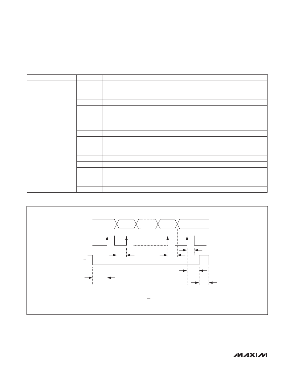
Figure 1. SPI Timing Diagram
FUNCTION
BIT
DESCRIPTION
Digital Attenuator State 2
(Path 1)
D17
16dB step (MSB of the 5-bit word used to program the Path 1 digital attenuator state 2)
D16
8dB step
D15
4dB step
D14
2dB step
D13
1dB step
Digital Attenuator State 1
(Path 1)
D12
16dB step (MSB of the 5-bit word used to program the Path 1 digital attenuator state 1)
D11
8dB step
D10
4dB step
D9
2dB step
D8
1dB step
On-Chip DAC
(Path 1)
D7
Bit 7 (MSB) of on-chip DAC used to program the Path 1 analog attenuator
D6
Bit 6 of DAC
D5
Bit 5 of DAC
D4
Bit 4 of DAC
D3
Bit 3 of DAC
D2
Bit 2 of DAC
D1
Bit 1 of DAC
D0 (LSB)
Bit 0 (LSB) of DAC
t
CS
MSB
LSB
DN
D1
D0
D(N-1)
t
CH
t
CW
t
ES
t
EW
t
EWS
DATA
CLOCK
CS
DATA ENTERED ON CLOCK RISING EDGE.
ATTENUATOR REGISTER STATE CHANGE ON CS RISING EDGE.
N = NUMBER OF DATA BITS.
NOTES: