Rainbow Electronics MAX2062 User Manual
Page 22
22 _____________________________________________________________________________________
MAX2062
Dual 50MHz to 1000MHz High-Linearity,
Serial/Parallel-Controlled Analog/Digital VGA
As an example, assume that the AGC application
requires a static attenuation adjustment to trim out gain
inconsistencies within a receiver lineup. The same AGC
circuit can also be called upon to dynamically attenu-
ate an unwanted blocker signal that could desensitize
the receiver and lead to an ADC overdrive condition.
In this example, the device would be preprogrammed
(through the SPI bus) with two customized attenuation
states—one to address the static gain-trim adjustment,
the second to counter the unwanted blocker condition.
Toggling just the STA_A_1 control bit enables the user to
switch quickly between the static and dynamic attenua-
tion settings with only one I/O pin.
If desired, the user can also program two additional
attenuation states by using the STA_B_1 control bit as a
second I/O pin. These two additional attenuation settings
are useful for software-defined radio applications where
multiple static gain settings are needed to account for dif-
ferent frequencies of operation, or where multiple dynamic
attenuation settings are needed to account for different
blocker levels (as defined by multiple wireless standards).
Power-Supply Sequencing
The sequence to be used is:
1) Power supply
2) Control lines
Layout Considerations
The pin configuration of the device is optimized to facili-
tate a very compact physical layout of the device and its
associated discrete components. The exposed pad (EP)
of the device’s 48-pin TQFN-EP package provides a low
thermal-resistance path to the die. It is important that
the PCB on which the device is mounted be designed
to conduct heat from the EP. In addition, provide the EP
with a low inductance path to electrical ground. The EP
MUST be soldered to a ground plane on the PCB, either
directly or through an array of plated via holes. The lay-
out of the PCB should include proper top-layer ground
shielding to isolate the amplifier’s inputs and outputs
from each other. Shielding between the paths (inputs and
outputs) is important for channel-to-channel isolation.
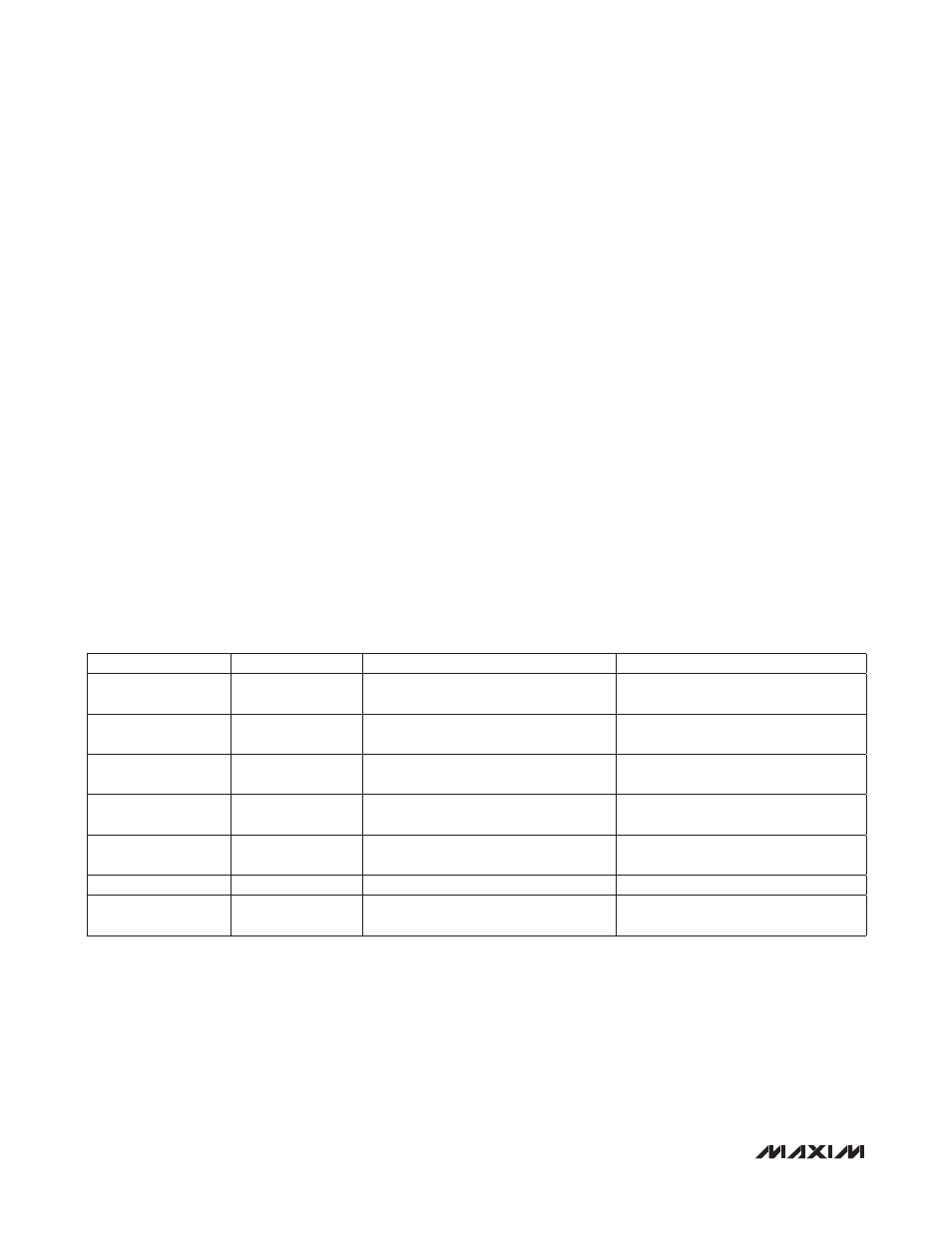
Table 7. Typical Application Circuit Component Values
*Select the inductors to ensure that self-resonance of the inductors is outside the band of operation.
DESIGNATION
QTy
DESCRIPTION
COMPONENT SUPPLIER
C1, C2, C5, C6, C8,
C9, C12, C13
8
1000pF ceramic capacitors (0402)
GRM1555C1H102J
Murata Electronics North America, Inc.
C3, C10
2
150pF ceramic capacitors (0402)
GRM1555C1H151J
Murata Electronics North America, Inc.
C4, C7, C11,
C14, C16
5
10nF ceramic capacitors (0402)
GRM155R71E103K
Murata Electronics North America, Inc.
C15
1
1FF ceramic capacitor (0603)
GRM188R71C105K
Murata Electronics North America, Inc.
L1, L2*
2
820nH inductors (1008)
Coilcraft 1008CS-821XJLC
Coilcraft, Inc.
R1, R2
2
47.5kI resistors (0402)
—
U1
1
48 TQFN-EP (7mm x 7mm)
Maxim MAX2062ETM
Maxim Integrated Products, Inc.