Typical operating characteristics (continued), Pin description – Rainbow Electronics MAX513 User Manual
Page 8
MAX512/MAX513
Low-Cost, Triple, 8-Bit Voltage-Output DACs
with Serial Interface
8
_______________________________________________________________________________________
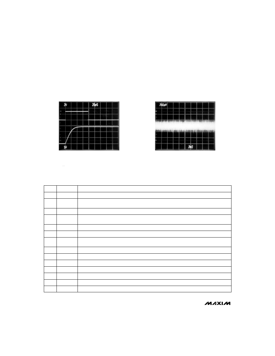
A
TIME EXITING SHUTDOWN MODE
20
µ
s/div
V
DD
= 3V, V
SS
= 0V, REFAB = V
DD,
R
L
= 1k
Ω
, C
L
= 0.1
µ
F
DAC LOADED WITH ALL 1s
B
A: CS, 2V/div
B: OUTA, 1V/div
_____________________________Typical Operating Characteristics (continued)
(T
A
= +25°C, unless otherwise noted.)
OUTA,
200
µ
V/div
OUTPUT VOLTAGE NOISE DC TO 1MHz
2ms/div
DIGITAL CODE = 80, REFAB = V
DD,
NO LOAD
______________________________________________________________Pin Description
DAC B Output Voltage (Buffered). Resets to full scale.
Connect 0.01µF capacitor or greater to GND.
OUTB
9
DAC C Output Voltage (Unbuffered). Resets to zero.
OUTC
10
DAC C Reference Voltage
REFC
11
DAC A/B Reference Voltage
REFAB
12
Internally connected. Do not make connections to this pin.
I.C.
13
Positive Power Supply (2.7V to 5.5V). Bypass with 0.22µF to GND.
V
DD
5
Ground
GND
6
Negative Power Supply 0V or (-1.5V to -5.5V). Tie to GND for single supply operation. If a negative supply
is applied, bypass with 0.22µF to GND.
V
SS
7
DAC A Output Voltage (Buffered). Resets to full scale.
Connect 0.1µF capacitor or greater to GND.
OUTA
8
Asynchronous reset input (active low). Clears all registers to their default state (FFhex for DAC A and
DAC B registers); all other registers are reset to 0 (including the input shift register).
–
R
—
E
—
S
—
E
—
T
–
4
Serial Clock Input. Data is clocked in on the rising edge of SCLK.
SCLK
3
PIN
Chip Select (active low). Enables data to be shifted into the 16-bit shift register. Programming commands
are executed at the rising edge of
–
C
—
S
–
.
–
C
—
S
–
2
Serial Data Input of the 16-bit shift register. Data is clocked into the register on the rising edge of SCLK.
DIN
1
FUNCTION
NAME
14
LOUT
Logic Output (latched)