Table 1. input shift register – Rainbow Electronics MAX513 User Manual
Page 10
SDIN
SCLK
CS
Q2
Q1
SC
SB
SA
LC
LB
LA
D7
D6
D5
D4
D3
D2
D1
D0
OPTIONAL
INSTRUCTION
EXECUTED
(CONTROL BYTE)
(DATA BYTE)
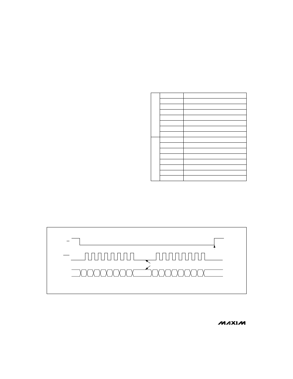
Figure 2. MAX512/MAX513 3-Wire Serial-Interface Timing Diagram
MAX512/MAX513
Low-Cost, Triple, 8-Bit Voltage-Output DACs
with Serial Interface
10
______________________________________________________________________________________
Shutdown Mode
When programmed to shutdown mode, the outputs of
DAC A and B go into a high-impedance state. Virtually
no current flows into or out of the buffer amplifiers in
that state. The output of DAC C goes to 0V when shut
down. In shutdown mode, the REF_ inputs are high
impedance (2M
Ω
typ) to conserve current drain from
the system reference; therefore, the system reference
does not have to be powered down. The logic output
LOUT remains active in shutdown.
Coming out of shutdown, the DAC outputs return to the
values kept in the registers. The recovery time is equiv-
alent to the DAC settling time.
Reset
The
–
R
—
E
—
S
—
E
—
T
–
input is active low. When asserted (
–
R
—
E
—
S
—
E
—
T
–
= 0), DACs A and B are set to full scale (FFhex) and
active, while DAC C is set to zero code (00hex) and
active. The 16-bit serial register is cleared to 0000hex.
LOUT is reset to zero.
Serial Interface
An active-low chip select (
–
C
—
S
–
) enables the shift register
to receive data from the serial data input. Data is
clocked into the shift register on every rising edge of
the serial clock signal (SCLK). The clock frequency can
be as high as 5MHz.
Data is sent MSB first and can be transmitted in one
16-bit word. The write cycle can be interrupted at any
time when
–
C
—
S
–
is kept active (low) to allow, for example,
two 8-bit-wide transfers. After clocking all 16 bits into
the input shift register, the rising edge of
–
C
—
S
–
updates
the DAC outputs, the shutdown status, and the status of
the logic output. Because of their single buffered struc-
ture, DACs cannot be simultaneously updated to differ-
ent digital values.
Table 1. Input Shift Register
*
*
Clocked in last.
**Clocked in first.
Uncommitted Bit
Q2**
Logic Output
Q1
Shut Down DAC C, Active High
SC
Shut Down DAC B, Active High
SB
Shut Down DAC A, Active High
SA
Load Reg DAC C, Active High
LC
Load Reg DAC B, Active High
LB
Load Reg DAC A, Active High
LA
DAC Data Bit 7 (MSB)
B7
DAC Data Bit 6
B6
DAC Data Bit 5
B5
DAC Data Bit 4
B4
DAC Data Bit 3
B3
DAC Data Bit 2
B2
DAC Data Bit 1
B1
DAC Data Bit 0 (LSB)
B0*
DATA BITS
CONTROL BITS