Applications information – Rainbow Electronics MAX513 User Manual
Page 12
MAX512/MAX513
Low-Cost, Triple, 8-Bit Voltage-Output DACs
with Serial Interface
12
______________________________________________________________________________________
_____________
Applications Information
Power-Supply and Reference
Operating Ranges
The MAX512 is fully specified to operate with
V
DD
= 5V ±10% and V
SS
= GND = 0V. The MAX513 is
specified for single-supply operation with V
DD
ranging from
2.7V to 3.6V, covering all commonly used supply voltages
in 3V systems. The MAX512/MAX513 can also be used
with a negative supply ranging from -1.5V to -5.5V. Using a
negative supply typically improves zero-code error and
settling time (as shown in the
Typical Operating
Characteristics graphs).
The two separate reference inputs for the DAC pair A/B
and the unbuffered output C allow different full-scale out-
put voltages and, if a negative supply is used, also allow
different polarity. In dual-supply mode, REFAB can vary
from V
SS
to (V
DD
- 1.5V). In single-supply mode, the
specified range for REFAB is 0V to V
DD
. REFC can range
from GND to V
DD
. Do not force REFC below ground.
Power-supply sequencing is not critical. If a negative sup-
ply is used, make sure V
SS
is never more than 0.3V above
ground. Do not apply signals to the digital inputs until the
device is powered-up. If this is not possible, add current-
limiting resistors to the digital inputs.
Power-Supply Bypassing and
Ground Management
In single-supply operation (V
SS
= GND), GND and V
SS
should be connected to the highest quality ground
available. Bypass V
DD
with a 0.1µF to 0.22µF capacitor
to GND. For dual-supply operation, bypass V
SS
with a
0.1µF to 0.22µF capacitor to GND. Reference inputs
can be used without bypassing. For optimum line/load-
transient response and noise performance, bypass the
reference inputs with 0.1µF to 4.7µF to GND. Careful
PC board layout minimizes crosstalk among DAC out-
puts, reference inputs, and digital inputs. Separate ana-
log lines with ground traces between them. Make sure
that high-frequency digital lines are not routed in paral-
lel to analog lines.
Unipolar Output
With unipolar output, the output voltage and the refer-
ence voltage are the same polarity. The MAX512/
MAX513 can be used with a single supply if the refer-
ence voltages are positive. With a negative supply,
t h e
REFAB voltage can vary from V
SS
to
approximately (V
DD
- 1.5V), allowing two-quadrant mul-
tiplication.
CS
SCLK
DIN
LOUT
t
DS
t
OD
t
DH
t
CL
t
CH
t
CSS
t
CSPWH
t
CSH
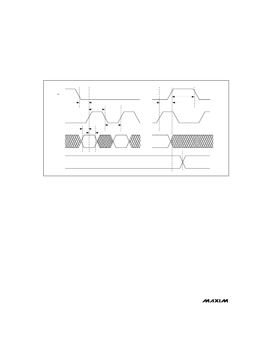
Figure 3. MAX512/MAX513 Detailed Serial-Interface Timing Diagram