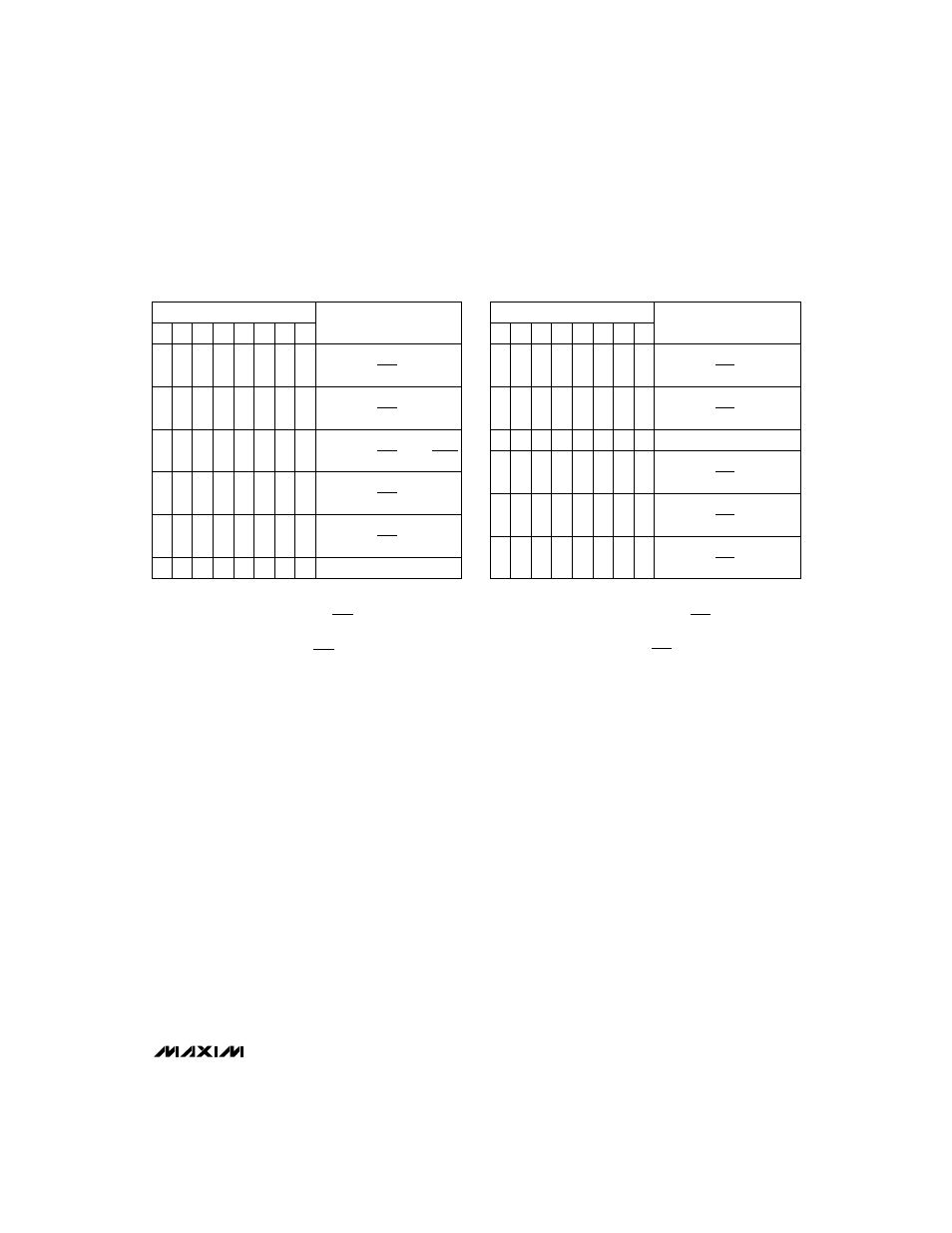
Table 3. unipolar code table, Table 4. bipolar code table – Rainbow Electronics MAX513 User Manual
Page 13
Bipolar Output
Using Figure 4’s circuit, the MAX512/MAX13 can be con-
figured for bipolar outputs. Table 4 lists the bipolar codes
and corresponding output voltages. There are two ways to
achieve rail-to-rail outputs: 1) Operate the
MAX512/MAX513 with a single supply and positive refer-
ence voltages or 2) Use dual supplies with a positive or
negative voltage at REFAB and a positive voltage at REFC.
In either case, the op amps need dual supplies. When
using the dual-supply mode, possible errors associated
with the divide-by-two attenuator and gain-of-two buffer are
eliminated (see the
Output Buffer Amplifier section). For
maximum output swing of all outputs in dual-supply mode,
connect REFAB to V
SS
and REFC to V
DD
. In single-supply
mode, connect REFAB, REFC, and V
DD
together.
With dual supplies, DACs A and B can perform four-
quadrant multiplication. Please note that in dual-supply
mode, the REFAB input ranges from V
SS
to (V
DD
-
1.5V). Because REFC accepts only positive inputs,
DAC C performs two-quadrant multiplication.
Figure 4 shows Maxim’s ICL7612A with rail-to-rail input
common-mode range and rail-to-rail output voltage
swing—ideal for a high output voltage swing from low
supply voltages.
RF Applications
Both the MAX512 and MAX513 can bias GaAs FETs,
where the gate of the FETs must be negatively biased
to ensure that there is no drain current. In a typical
application, power to the RF amplifiers should not be
turned on until the bias voltages provided by DAC A
and DAC B are fully established; likewise, the supply
should be turned off before the bias voltage is switched
off. Figure 5 shows how DAC B supplies the negative
bias V
GG1
for the driver stage and DAC A provides the
negative bias V
GG2
for the output stage [1].
The DAC A and DAC B outputs are also ideal for con-
trolling VCOs in mobile radios or cellular phones. Other
applications include varactor and PIN diode circuits.
The unbuffered DAC C provides a span within GND
and V
DD
and is individually set at REF C. DAC C typi-
cally adjusts offset and gain in the system.
1 [John Wachsmann. “A High-Efficiency GaAs MMIC Power Amplifier for
1.9GHz PCS Applications,” Proceedings of the First Annual Wireless
Symposium, pp. 375, Penton Publishing, Jan. 1993.]
MAX512/MAX513
Low-Cost, Triple, 8-Bit Voltage-Output DACs
with Serial Interface
______________________________________________________________________________________
13
DAC CONTENTS
B7 B6 B5 B4 B3 B2 B1 B0
ANALOG
OUTPUT
1
1
1
1
1
1
1
1
+
×
REF_
255
256
1
0
0
0
0
0
0
1
+
×
REF_
129
256
1
0
0
0
0
0
0
0
+
×
= +
REF_
128
256
REF_
2
0
1
1
1
1
1
1
1
+
×
REF_
127
256
0
0
0
0
0
0
0
1
+
×
REF_
1
256
0
0
0
0
0
0
0
0
0V
Note :
1LSB
REF_
2
REF_
1
256
ANALOG OUTPUT
REF_
D
256
8
=
Ч
=
Ч
=
Ч
−
Table 3. Unipolar Code Table
DAC CONTENTS
B7 B6 B5 B4 B3 B2 B1 B0
ANALOG
OUTPUT
1
1
1
1
1
1
1
1
+
×
REF_
127
128
1
0
0
0
0
0
0
1
+
×
REF_
1
128
0
1
1
1
1
1
1
1
−
×
REF_
1
128
0
0
0
0
0
0
0
1
−
×
REF_
127
128
0
0
0
0
0
0
0
0
−
×
−
REF_
128
128
= REF_
1
0
0
0
0
0
0
0
0V
Note :
1LSB
REF_
2
REF_
1
128
ANALOG OUTPUT
REF_
D
128
1
8 - 1)
=
Ч
=
Ч
=
Ч
−
−
(
Table 4. Bipolar Code Table