Rainbow Electronics MAX513 User Manual
Page 2
LSB
MAX512/MAX513
Low-Cost, Triple, 8-Bit Voltage-Output DACs
with Serial Interface
2
_______________________________________________________________________________________
ABSOLUTE MAXIMUM RATINGS
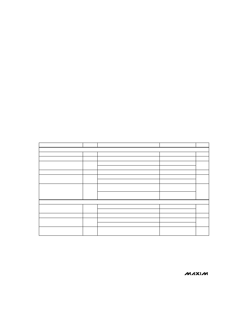
ELECTRICAL CHARACTERISTICS
(V
DD
= +4.5V to +5.5V for MAX512, V
DD
= +2.7V to +3.6V for MAX513, V
SS
= GND = 0V, REFAB = REFC = V
DD
,
T
A
= T
MIN
to T
MAX
, unless otherwise noted. Typical values are at T
A
= +25°C.)
Note 1:
The outputs may be shorted to V
DD
, V
SS
, or GND if the package power dissipation is not exceeded. Typical short-circuit cur-
rent to GND is 50mA.
Stresses beyond those listed under “Absolute Maximum Ratings” may cause permanent damage to the device. These are stress ratings only, and functional
operation of the device at these or any other conditions beyond those indicated in the operational sections of the specifications is not implied. Exposure to
absolute maximum rating conditions for extended periods may affect device reliability.
V
DD
to GND ................................................................ -0.3V, +6V
V
SS
to GND ................................................................. -6V, +0.3V
V
DD
to V
SS
................................................................ -0.3V, +12V
Digital Inputs and Outputs to GND............... -0.3V, (V
DD
+ 0.3V)
REFAB ................................................ (V
SS
- 0.3V), (V
DD
+ 0.3V)
OUTA, OUTB (Note 1) ....................................................V
SS
, V
DD
OUTC.............................................................-0.3V, (V
DD
+ 0.3V)
REFC..............................................................-0.3V, (V
DD
+ 0.3V)
Continuous Power Dissipation (T
A
= +70°C)
Plastic DIP (derate 10.00mW/°C above +70°C) ............800mW
SO (derate 8.33mW/°C above +70°C) ...........................667mW
CERDIP (derate 9.09mW/°C above +70°C) ...................727mW
Operating Temperature Ranges
MAX51_C_ _ .........................................................0°C to +70°C
MAX51_E_ _.......................................................-40°C to +85°C
MAX51_MJD ....................................................-55°C to +125°C
Storage Temperature Range .............................-65°C to +165°C
Lead Temperature (soldering, 10sec) .............................+300°C
REFAB, REFC
REFC (Note 3)
REFAB (Note 3)
REFC
REFAB
MAX513, 2.7V
≤
V
DD
≤
3.6V,
REFAB = REFC = 2.4V
MAX512, 4.5V
≤
V
DD
≤
5.5V,
REFAB = REFC = 4.096V
DAC C
DAC A/B
CONDITIONS
M
Ω
2
Reference Input Resistance
(shutdown mode)
k
Ω
12
R
REF
Reference Input Resistance
8
pF
25
Reference Input Capacitance
V
GND
V
DD
Reference Input Voltage Range
V
SS
V
DD
%/%
0.01
PSRR
Power-Supply Rejection Ratio
Bits
8
N
Resolution
µV/°C
5
Zero-Code Temperature
Coefficient
100
UNITS
MIN
TYP
MAX
SYMBOL
PARAMETER
Guaranteed monotonic
LSB
±1
DNL
Differential Nonlinearity
0.015
DAC A/B (Note 2)
LSB
±1.5
INL
Integral Nonlinearity
(Note 2)
LSB
±1
TUE
Total Unadjusted Error
DAC C
±1
STATIC PERFORMANCE
REFERENCE INPUTS