Ac electrical characteristics (continued) – Rainbow Electronics MAX108 User Manual
Page 5
MAX108
±5V, 1.5Gsps, 8-Bit ADC with
On-Chip 2.2GHz Track/Hold Amplifier
_______________________________________________________________________________________
5
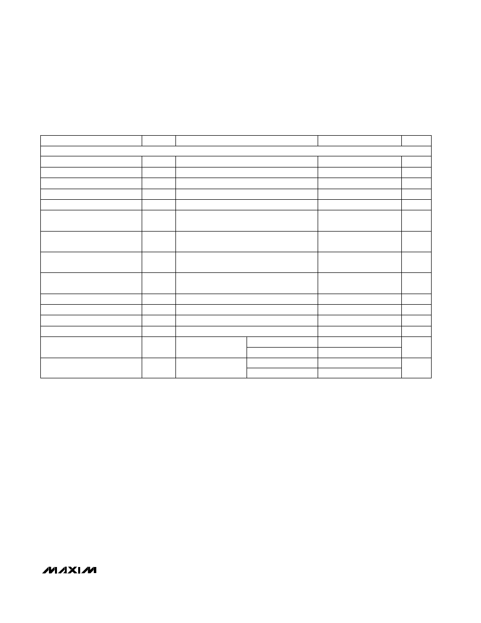
AC ELECTRICAL CHARACTERISTICS (continued)
(V
CC
A = V
CC
I = V
CC
D = +5.0V, V
EE
= -5.0V, V
CC
O = +3.3V, REFIN connected to REFOUT, f
S
= 1.5Gsps, f
IN
at -1dBFS, T
A
= +25°C,
unless otherwise noted.)
DIV4 mode
DIV1, DIV2 modes
7.5
DIV4 mode
DIV1, DIV2 modes
Figures 6, 7, 8
t
PDP
Auxiliary Port Pipeline
Delay
t
PDA
9.5
Clock
Cycles
Figures 6, 7, 8
8.5
DREADY to DATA Propagation
Delay (Note 14)
t
PD2
-50
150
350
ps
Figure 17
CLK to DREADY Propagation
Delay
t
PD1
2.2
ns
Figure 17
Reset Input Data Hold Time
(Note 13)
t
HD
0
ps
Figure 15
Clock Pulse Width High
t
PWH
0.3
5
ns
Figure 17
PARAMETER
SYMBOL
MIN
TYP
MAX
UNITS
Aperture Jitter
t
AJ
<0.5
ps
Aperture Delay
t
AD
100
ps
Reset Input Data Setup Time
(Note 13)
t
SU
0
ps
DATA Rise Time
t
RDATA
420
ps
Maximum Sample Rate
f
MAX
1.5
Gsps
Clock Pulse Width Low
t
PWL
0.3
ns
DATA Fall Time
t
FDATA
360
ps
DREADY Rise Time
t
RDREADY
220
ps
DREADY Fall Time
t
FDREADY
180
ps
Primary Port Pipeline
Delay
7.5
Clock
Cycles
CONDITIONS
Figure 4
Figure 4
Figure 15
20% to 80%, C
L
= 3pF
20% to 80%, C
L
= 3pF
20% to 80%, C
L
= 3pF
20% to 80%, C
L
= 3pF
Figure 17
TIMING CHARACTERISTICS
Note 1:
Static linearity parameters are computed from a “best-fit” straight line through the code transition points. The full-scale
range (FSR) is defined as 256 times the slope of the line.
Note 2:
The offset control input is a self-biased voltage divider from the internal +2.5V reference voltage. The nominal open-circuit
voltage is +1.25V. It may be driven from an external potentiometer connected between REFOUT and GNDI.
Note 3:
The clock input’s termination voltage can be operated between -2.0V and GNDI. Observe the absolute maximum ratings
on the CLK+ and CLK- inputs.
Note 4:
Input logic levels are measured with respect to the V
CC
O power-supply voltage.
Note 5:
All PECL digital outputs are loaded with 50
Ω
to V
CC
O - 2.0V. Measurements are made with respect to the V
CC
O power-
supply voltage.
Note 6:
The current in the V
CC
O power supply does not include the current in the digital output’s emitter followers, which is a func-
tion of the load resistance and the V
TT
termination voltage.
Note 7:
Common-mode rejection ratio (CMRR) is defined as the ratio of the change in the transfer-curve offset voltage to the
change in the common-mode voltage, expressed in dB.
Note 8:
Power-supply rejection ratio (PSRR) is defined as the ratio of the change in the transfer-curve offset voltage to the change
in power-supply voltage, expressed in dB.
Note 9:
Measured with the positive supplies tied to the same potential; V
CC
A = V
CC
D = V
CC
I. V
CC
varies from +4.75V to +5.25V.
Note 10:
V
EE
varies from -5.25V to -4.75V.