Rainbow Electronics MAX194 User Manual
Page 2
MAX194
14-Bit, 85ksps ADC with 10µA Shutdown
2
_______________________________________________________________________________________
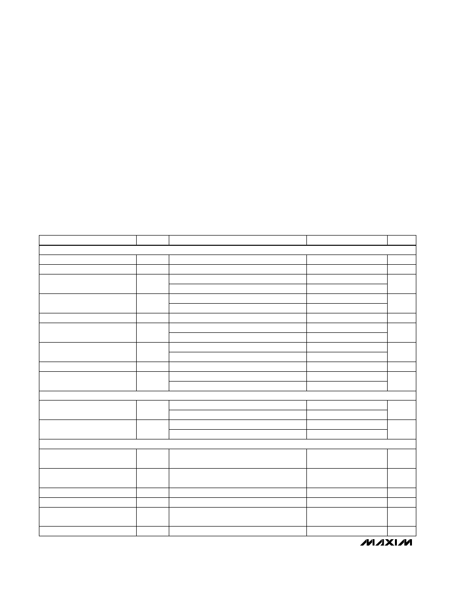
ABSOLUTE MAXIMUM RATINGS
ELECTRICAL CHARACTERISTICS
(VDDD = VDDA = +5V, VSSD = VSSA = -5V, f
CLK
= 1.7MHz, V
REF
= +5V, T
A
= T
MIN
to T
MAX
, unless otherwise noted. Typical
values are at T
A
= +25°C.)
Stresses beyond those listed under “Absolute Maximum Ratings” may cause permanent damage to the device. These are stress ratings only, and functional
operation of the device at these or any other conditions beyond those indicated in the operational sections of the specifications is not implied. Exposure to
absolute maximum rating conditions for extended periods may affect device reliability.
VDDD to DGND .....................................................................+7V
VDDA to AGND......................................................................+7V
VSSD to DGND.........................................................+0.3V to -6V
VSSA to AGND .........................................................+0.3V to -6V
VDDD to VDDA, VSSD to VSSA ..........................................±0.3V
AIN, REF ....................................(VSSA - 0.3V) to (VDDA + 0.3V)
AGND to DGND ..................................................................±0.3V
Digital Inputs to DGND...............................-0.3V, (VDDA + 0.3V)
Digital Outputs to DGND............................-0.3V, (VDDA + 0.3V)
Continuous Power Dissipation (T
A
= +70°C)
Plastic DIP (derate 10.53mW/°C above +70°C) ............842mW
Wide SO (derate 9.52mW/°C above +70°C)..................762mW
Ceramic SB (derate 10.53mW/°C above +70°C)...........842mW
Operating Temperature Ranges
MAX194_C_E ........................................................0°C to +70°C
MAX194_E_E .....................................................-40°C to +85°C
MAX194_MDE..................................................-55°C to +125°C
Storage Temperature Range .............................-65°C to +160°C
Lead Temperature (soldering, 10sec) .............................+300°C
16(t
CLK
)
Unipolar
MAX194B, V
REF
= 4.75V
MAX194A, V
REF
= 4.75V
MAX194A
MAX194B
MAX194A, V
REF
= 4.75V
VSSA = -5.25V to -4.75V, V
REF
= 4.75V
MAX194B, V
REF
= 4.75V
VDDA = 4.75V to 5.25V, V
REF
= 4.75V
CONDITIONS
MHz
1.7
f
CLK
Clock Frequency
(Notes 2, 3)
µs
9.4
t
CONV
Conversion Time
dB
-90
Peak Spurious Noise
dB
-90
THD
Total Harmonic Distortion
(up to the 5th harmonic)
V
0
V
REF
Input Range
dB
65
Power-Supply Rejection
Ratio (VDDA and VSSA only)
65
LSB
±1
DNL
Differential Nonlinearity
Bits
14
RES
Resolution
ppm/°C
0.1
Full-Scale Tempco
LSB
±2
Unipolar Full-Scale Error
±1
Unipolar/Bipolar Offset Tempco
ppm/°C
0.4
±1⁄2
LSB
±1
INL
Integral Nonlinearity
±1
LSB
±2
Unipolar/Bipolar Offset Error
UNITS
MIN
TYP
MAX
SYMBOL
PARAMETER
Unipolar
pF
250
Input Capacitance
dB
82
SINAD
Signal-to-Noise plus Distortion
Ratio
MHz
5
f
SCLK
Serial Clock Frequency
Bipolar
Bipolar
125
-V
REF
V
REF
MAX194B, V
REF
= 4.75V
MAX194A, V
REF
= 4.75V
LSB
±4
Bipolar Full-Scale Error
±2
ACCURACY
(Note 1)
ANALOG INPUT
DYNAMIC PERFORMANCE
(f
s
= 85kHz, bipolar range AIN = -5V to +5V, 1kHz) (Note 1)