Max194, Bit, 85ksps adc with 10µa shutdown – Rainbow Electronics MAX194 User Manual
Page 10
MAX194
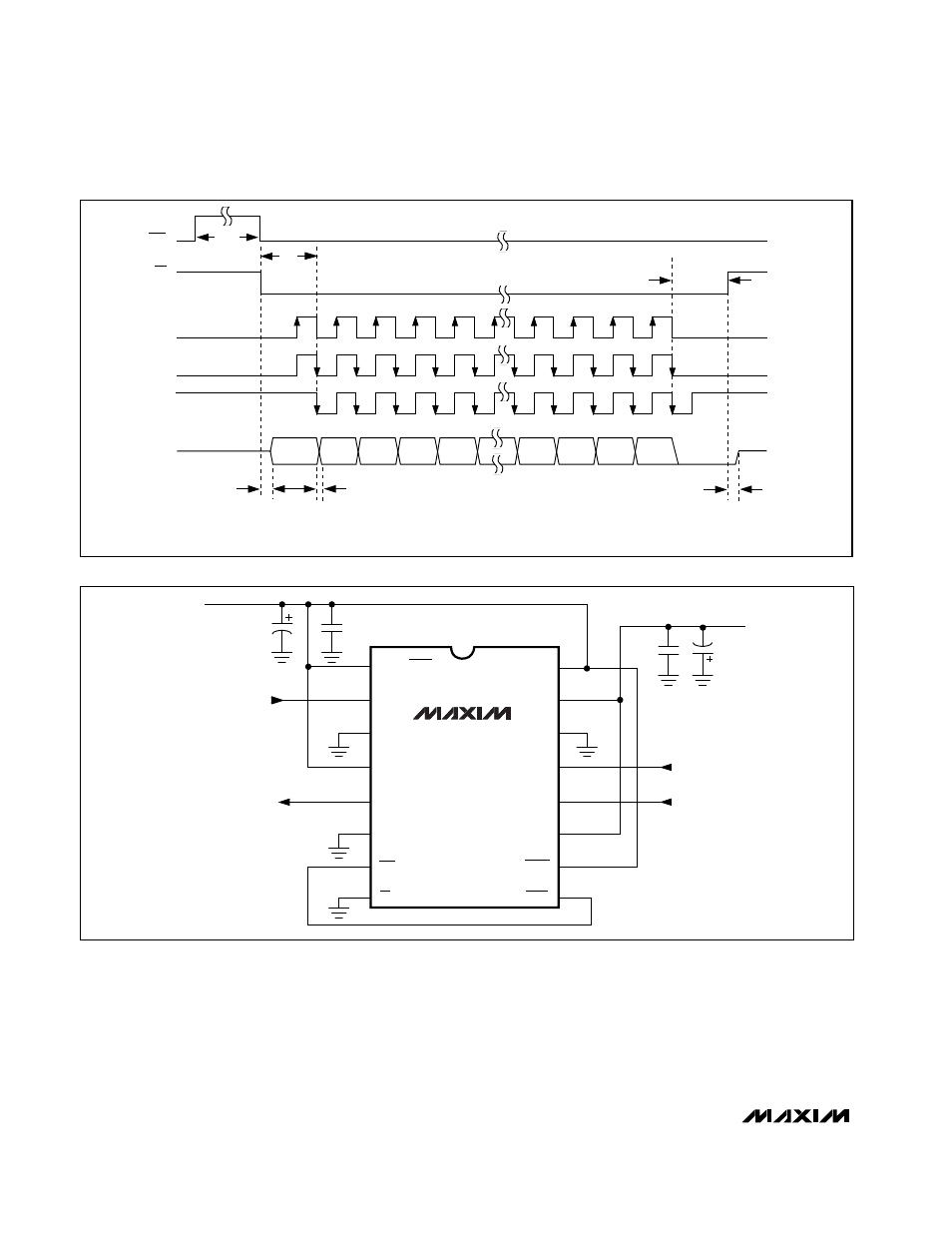
mum (1.7MHz), reading the data after each conversion
(during the acquisition time) results in lower throughput
(about 70ksps max) than reading the data during con-
versions, because it takes longer than the minimum
input acquisition time (four cycles at 1.7MHz) to clock
16 data bits at 5Mbps. After the data has been clocked
in, leave some time (about 1µs) for any coupled noise
on AIN to settle before beginning the next conversion.
Whichever method is chosen for reading the data, con-
versions can be individually initiated by bringing CONV
low, or they can occur continuously by connecting EOC
to CONV. Figure 8 shows the MAX194 in its simplest
operational configuration.
14-Bit, 85ksps ADC with 10µA Shutdown
10
______________________________________________________________________________________
EOC
CS
SCLK
(CASE 1)
SCLK
(CASE 2)
CASE 1: SCLK IDLES LOW, DATA LATCHED ON RISING EDGE (CPOL = 0, CPHA = 0)
CASE 2: SCLK IDLES LOW, DATA LATCHED ON FALLING EDGE (CPOL = 0, CPHA = 1)
CASE 3: SCLK IDLES HIGH, DATA LATCHED ON FALLING EDGE (CPOL = 1, CPHA = 0)
NOTE: ARROWS ON SCLK TRANSITIONS INDICATE LATCHING EDGE
DOUT
SCLK
(CASE 3)
t
CONV
t
DH
t
SD
t
DV
MSB
LSB
SUB-LSBs
B13
B12
B11
B10
B1
B0
S1
S0
B9
t
CSS
t
CSH
MAX194
10
µ
F
BP/UP/SHDN
CLK
SCLK
VDDD
DOUT
DGND
REFERENCE (0V TO VDDA)
ANALOG INPUT
-5V
EOC
CS
VDDA
VSSA
AGND
AIN
CONVERSION CLOCK
+5V
REF
VSSD
RESET
CONV
0.1
µ
F
10
µ
F
0.1
µ
F
1
2
3
4
5
6
7
8
16
15
14
13
12
11
10
9
Figure 7. Output Data Format, Reading Data Between Conversions (Mode 2)
Figure 8. MAX194 in the Simplest Operating Configuration