Rainbow Electronics MAX194 User Manual
Page 17
Data is clocked out of the MAX194 on CLK’s falling
edge and can be clocked into the µP on the rising
edge or the following falling edge. If you clock data in
on the rising edge (SPI/QSPI with CPOL = 0 and CPHA
= 0; standard MicroWire™: Hitachi H8), the maximum
CLK rate is given by:
where t
CD
is the MAX194’s CLK-to-DOUT valid delay
and t
SD
is the data setup time for your µP.
If clocking data in on the falling edge (CPOL = 0,
CPHA = 1), the maximum CLK rate is given by:
Do not exceed the maximum CLK frequency given in
the
Electrical Characteristics
table. To clock data in on
the falling edge, your processor hold time must not
exceed t
CD
minimum (100ns).
While QSPI can provide the required 20 CLK cycles as
two continuous 10-bit transfers, SPI is limited to 8-bit
transfers. This means that with SPI, a conversion must
consist of three 8-bit transfers. Ensure that the pauses
between 8-bit operations at your selected clock rate
are short enough to maintain a 20ms or shorter conver-
sion time, or the leakage of the capacitive DAC may
cause errors.
f
=
1
t
+ t
CLK(max)
CD
SD
f
= /
1
t
+ t
CLK(max)
1
2
CD
SD
•
MAX194
14-Bit, 85ksps ADC with 10µA Shutdown
______________________________________________________________________________________
17
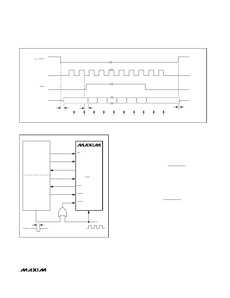
EOC
CLK
t
CD
t
DV
DATA LATCHED:
t
DH
CS, CONV
DOUT
B13 FROM PREVIOUS
CONVERSION
B13
B13
B0
B12
S1
S0
MAX194
QSPI
GPT
BP/UP/SHDN
SCLK
EOC
DOUT
RESET
CONV
1.7MHz
CLK
IC3
CS
OC3
SCK
IC1
MISO
OC2
START
PCS0
1.3
µ
s
74HC32
Figure 19. MAX194 Connection to QSPI Processor Clocking
Data Out with SCLK Between Conversions
Figure 18. Timing Diagram for Circuit of Figure 17
MicroWire is a trademark of National Semiconductor Corp.