Pc board layout guidelines – Rainbow Electronics MAX1813 User Manual
Page 36
MAX1813
Dynamically-Adjustable, Synchronous Step-Down
Controller with Integrated Voltage Positioning
36
______________________________________________________________________________________
about 2-3% at 600kHz when compared to the 300kHz
voltage-positioned circuit, primarily due to the high-side
MOSFET switching losses.
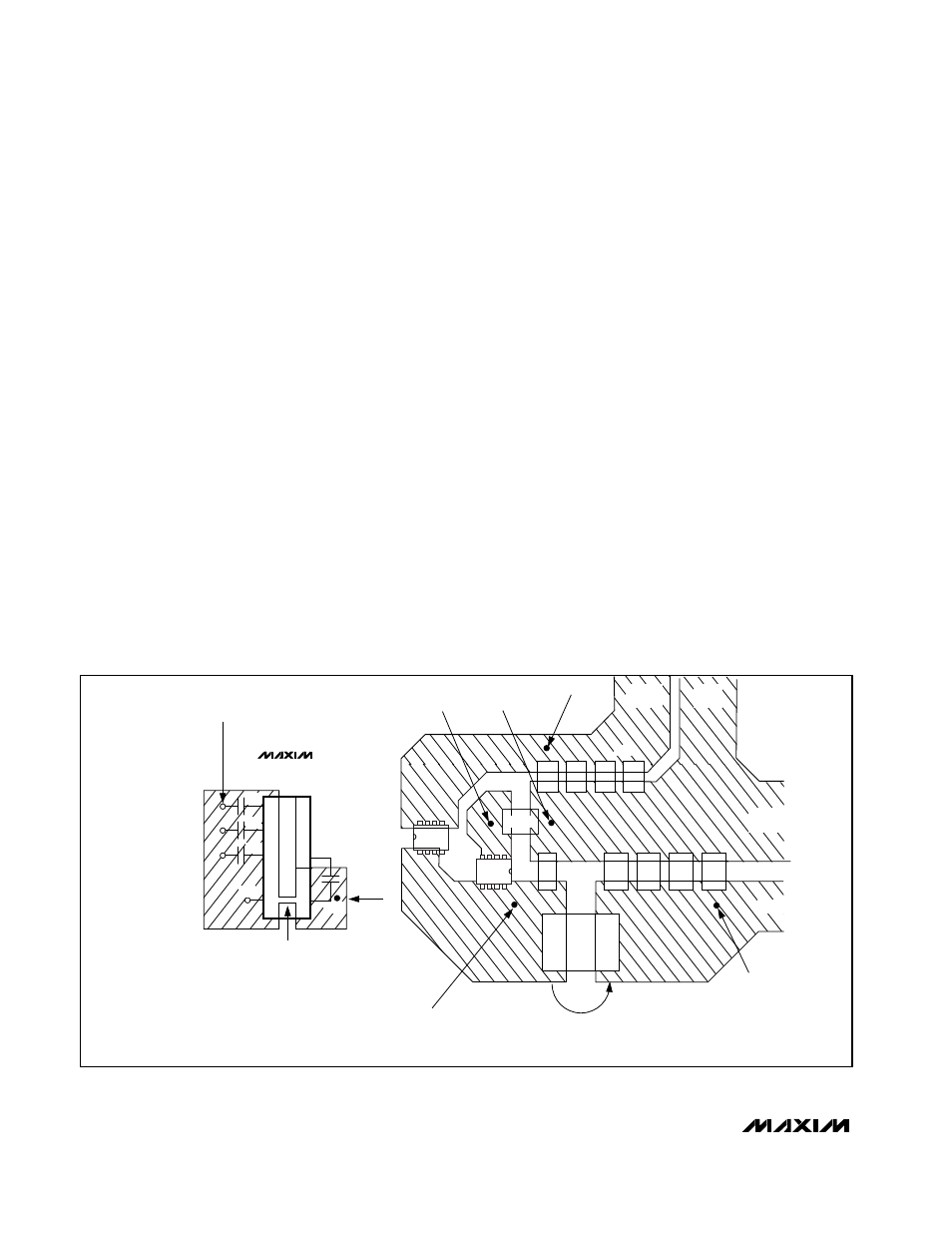
PC Board Layout Guidelines
Careful PC board layout is critical to achieve low
switching losses and clean, stable operation. The
switching power stage requires particular attention
(Figure 19). If possible, mount all of the power compo-
nents on the top side of the board, with their ground
terminals flush against one another. Follow these guide-
lines for good PC board layout:
1) Keep the high-current paths short, especially at the
ground terminals. This is essential for stable, jitter-
free operation.
2) Connect all analog grounds to a separate solid cop-
per plane, which connects to the MAX1813’s GND
pin. This includes the V
CC
, REF, and CC capacitors,
as well as the resistive-dividers connected to FB
and ILIM.
3) Keep the power traces and load connections short.
This is essential for high efficiency. The use of thick
copper PC boards (2oz vs. 1oz) can enhance full-
load efficiency by 1% or more. Correctly routing PC
board traces is a difficult task that must be
approached in terms of fractions of centimeters,
where a single m
Ω of excess trace resistance caus-
es a measurable efficiency penalty.
4) VPCS and GND connections for current limiting and
voltage positioning must be made using Kelvin
sensed connections to guarantee the current-sense
accuracy.
5) When trade-offs in trace lengths must be made, it’s
preferable to allow the inductor charging path to be
made longer than the discharge path. For example,
it’s better to allow some extra distance between the
input capacitors and the high-side MOSFET than to
allow distance between the inductor and the low-
side MOSFET or between the inductor and the out-
put filter capacitor.
6) Ensure the FB connection to the output is short and
direct.
7) Route high-speed switching nodes away from sensi-
tive analog areas (CC, REF, ILIM). Make all pin-strap
control input connections (SKP/SDN, ILIM, CODE,
SUS, ZMODE, etc.) to analog ground or V
CC
rather
than power ground (PGND) or V
DD
.
D1
VIA TO V+
VIA TO LX
VIA TO FB
VIA TO
SOURCE
OF Q2
VIA TO GND
NEAR R
SENSE
VIA TO VPCS
INDUCTOR DISCHARGE PATH HAS LOW DC RESISTANCE.
V
DD
ALL ANALOG GROUNDS
CONNECT TO LOCAL PLANE ONLY
NOTES: “STAR” GROUND IS USED.
D1 IS DIRECTLY ACROSS Q2.
CONNECT LOCAL ANALOG GROUND PLANE DIRECTLY TO GND FROM
THE SIDE OPPOSITE THE V
DD
CAPACITOR GND TO AVOID V
DD
GROUND
CURRENTS FROM FLOWING IN THE ANALOG GROUND PLANE.
MAX1813
;
;
BATTERY
INPUT
L1
V
OUT
Q2
Q1
R
SENSE
D1
GND
INPUT
GND
OUTPUT
PGND
GND
V
CC
CC
REF
C
OUT
C
IN
Figure 19. Power-Stage PC Board Layout Example