Rainbow Electronics MAX1813 User Manual
Page 2
MAX1813
Dynamically-Adjustable, Synchronous Step-Down
Controller with Integrated Voltage Positioning
2
_______________________________________________________________________________________
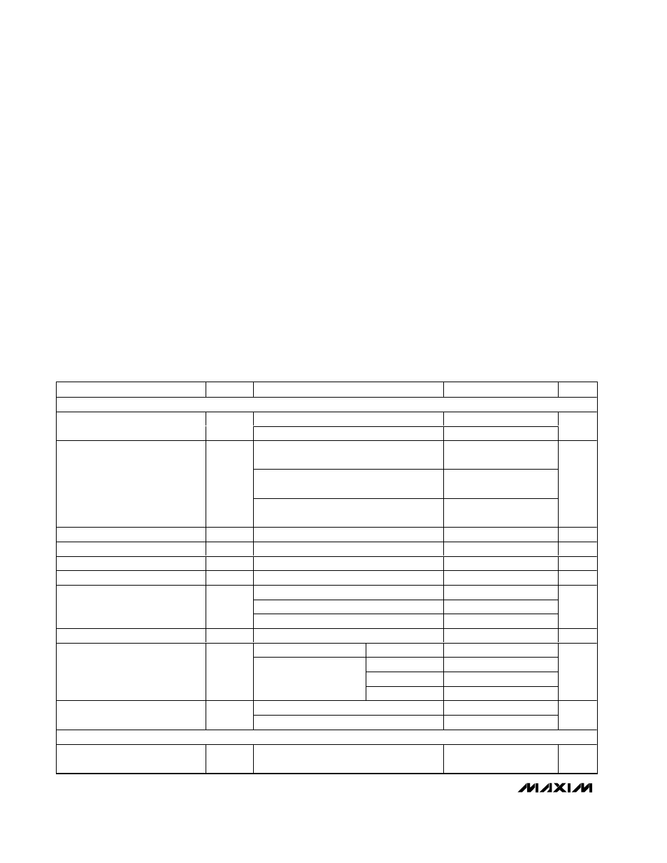
ABSOLUTE MAXIMUM RATINGS
ELECTRICAL CHARACTERISTICS
(Circuit of Figure 1, V+ = +15V, V
CC
= V
DD
= 5V, VPCS = ZMODE = GND = PGND, SKP/SDN = CODE = V
CC
, V
OUT
set to 1.5V,
T
A
= 0
°C to +85°C, unless otherwise noted. Typical values are at T
A
= +25
°C.)
Stresses beyond those listed under “Absolute Maximum Ratings” may cause permanent damage to the device. These are stress ratings only, and functional
operation of the device at these or any other conditions beyond those indicated in the operational sections of the specifications is not implied. Exposure to
absolute maximum rating conditions for extended periods may affect device reliability.
Note 1: SKP/SDN may be forced to 12V, temporarily exceeding the absolute maximum rating, for the purpose of debugging proto-
type breadboards, using the no-fault test mode.
V+ to GND ..............................................................-0.3V to +30V
V
CC
, V
DD
to GND .....................................................-0.3V to +6V
PGND to GND.....................................................................±0.3V
D0–D4, CODE, ZMODE, SUS, PGOOD to GND ......-0.3V to +6V
SKP/SDN to GND (Note 1) .....................................-0.3V to +16V
ILIM, FB, CC, REF,
TON, TIME, S0, S1 to GND......................-0.3V to (V
CC
+ 0.3V)
VPCS to GND ............................................................-2V to +30V
DL to PGND................................................-0.3V to (V
DD
+ 0.3V)
BST to PGND..........................................................-0.3V to +36V
DH to LX ....................................................-0.3V to (V
BST
+ 0.3V)
LX to BST..................................................................-6V to +0.3V
REF Short Circuit to GND ...........................................Continuous
Continuous Power Dissipation (T
A
= +70
°C)
28-Pin QSOP (derate 10.8mW/
°C above +70°C)..........860mW
Operating Temperature Range ...........................-40
°C to +85°C
Junction Temperature ......................................................+150
°C
Storage Temperature Range .............................-65
°C to +150°C
Lead Temperature (soldering, 10s) .................................+300
°C
PARAMETER
SYMBOL
CONDITIONS
MIN
TYP
MAX
UNITS
PWM CONTROLLER
Battery voltage, V+
2
28
Input Voltage Range
V
CC
, V
DD
4.5
5.5
V
V+ = 4.5V to 28V, VPCS = GND, DAC
codes from 0.925V to 2.0V
-1
+1
V+ = 4.5V to 28V, VPCS = GND, DAC
codes from 0.700V to 0.900V
-1.5
+1.5
DC Output Voltage Accuracy
(Notes 2, 3)
V+ = 4.5V to 28V, VPCS = GND, DAC
codes from 0.600V to 0.675V
-1.83
+1.83
%
VPCS Input Bias Current
I
VPS
V
VPCS
= 0 or 28V
-1
+1
µA
VPCS Transconductance
G
m
V
VPCS
= 0 to -100mV
18
20
22
µS
VPCS Linear Input Range
±100
mV
FB Input Resistance
R
FB
115
180
265
k
Ω
38kHz nominal, R
TIME
= 470k
Ω
-12
+12
150kHz nominal, R
TIME
= 120k
Ω
-8
+8
TIME Frequency Accuracy
380kHz nominal, R
TIME
= 47k
Ω
-12
+12
%
ILIM Input Leakage Current
I
ILIM
V
ILIM
= 0 or 5.0V
0.01
100
nA
V+ = 5.0V, V
FB
= 1.2V
TON = GND
250
270
290
TON = REF
165
190
215
TON = open
320
355
390
On-Time (Note 4)
t
ON
V+ = 12V, V
FB
= 1.2V
TON = V
CC
465
515
563
ns
TON = REF, open, or V
CC
400
500
Minimum Off-Time (Note 4)
t
OFF(MIN)
TON = GND
300
375
ns
BIAS AND REFERENCE
Quiescent Supply Current (V
CC
)
I
CC
Measured at V
CC
, FB forced above the
regulation point
1.4
2.5
mA