Rainbow Electronics MAX1401 User Manual
Page 21
MAX1401
+3V, 18-Bit, Low-Power, Multichannel,
Oversampling (Sigma-Delta) ADC
______________________________________________________________________________________
21
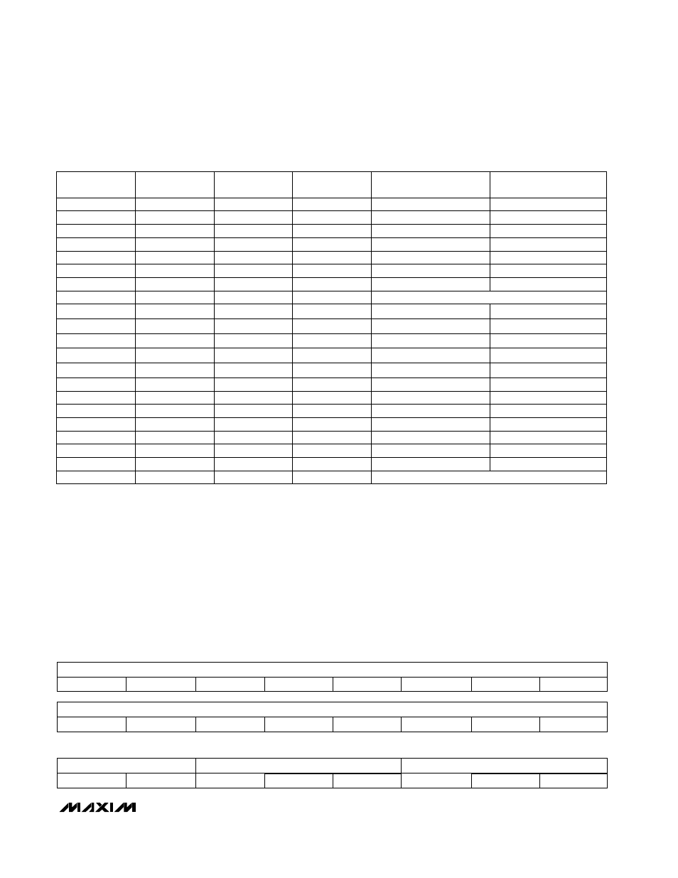
Table 10. Transfer-Function Register Mapping—Gain-Calibration Mode (M1 = 1, M0 = 0)
X = Don’t care
First Bit (Data MSB)
RESERVED BITS
CHANNEL ID TAG
D1
‘0’
D0
‘0’
‘0’
CID0
DATA BITS
CID2
CID1
D9
D5
D8
D7
D6
D2
DATA BITS
D4
D3
(Data LSB)
(LSB)
D17
D13
D16
D15
D14
D10
DATA BITS
D12
D11
0
DIFF
0
A1
0
0
1
0
0
1
0
1
2
0
2
1
0
0
0
X
0
X
1
1
0
X
0
X
2
1
2
1
1
1
1
0
1
0
2
SCAN
0
1
1
TRANSFER-
FUNCTION REGISTER
1
X
1
X
3
1
0
0
0
X
0
X
3
1
0
X
1
X
1
1
3
3
1
1
0
A0
1
0
1
X
X
X
X
0
1
0
3
X
X
X
X
CALGAIN+–CALGAIN-
CALGAIN+–CALGAIN-
CALGAIN+–CALGAIN-
CALGAIN+–CALGAIN-
AIN2–AIN6
AIN4–AIN6
AIN3–AIN6
AIN1–AIN6
CALGAIN+–CALGAIN-
CHANNEL
1
CALGAIN+–CALGAIN-
CALGAIN+–CALGAIN-
CALOFF+–CALOFF-
AIN1–AIN2
CALGAIN+–CALGAIN-
AIN5–AIN6
1
X
1
X
3
1
3
2
1
1
X
X
X
X
AIN5–AIN6
CALGAIN+–CALGAIN-
CALOFF+–CALOFF-
AIN3–AIN4
1
1
Do Not Use
0
1
1
1
Do Not Use
1
1
Data Register (Read-Only)
The data register is a 24-bit, read-only register. Any
attempt to write data to this location will have no effect.
If a write operation is attempted, 8 bits of data must be
clocked into the part before it will return to its normal
idle mode, expecting a write to the communications
register.
Data is output MSB first, followed by three reserved 0
bits and a 3-bit channel ID tag indicating the channel
from which the data originated.
D17–D0:
The conversion result. D17 is the MSB. The
result is in offset binary format. 00 0000 0000 0000
0000 represents the minimum value and 11 1111 1111
1111 1111 represents the maximum value. Inputs
exceeding the available input range are limited to the
corresponding minimum or maximum output values.
0:
These reserved bits will always be 0.
CID2–0:
Channel ID tag (Table 11).
Data Register (Read-Only) Bits