Rainbow Electronics MAX1401 User Manual
Page 16

MAX1401
+3V, 18-Bit, Low-Power, Multichannel,
Oversampling (Sigma-Delta) ADC
16
______________________________________________________________________________________
FSYNC:
(Default = 0) Filter Sync Bit. When FSYNC = 0,
conversions are automatically performed at a data rate
determined by CLK, FS1, FS0, MF1, and MF0 bits.
When FSYNC = 1, the digital filter and analog modulator
are held in reset, inhibiting normal self-timed operation.
This bit may be used to convert on command to mini-
mize the settling time to valid output data, or to synchro-
nize operation of a number of MAX1401s. FSYNC does
not reset the serial interface or the 0/DRDY flag. To clear
the 0/DRDY flag while FSYNC is active, simply read the
data register.
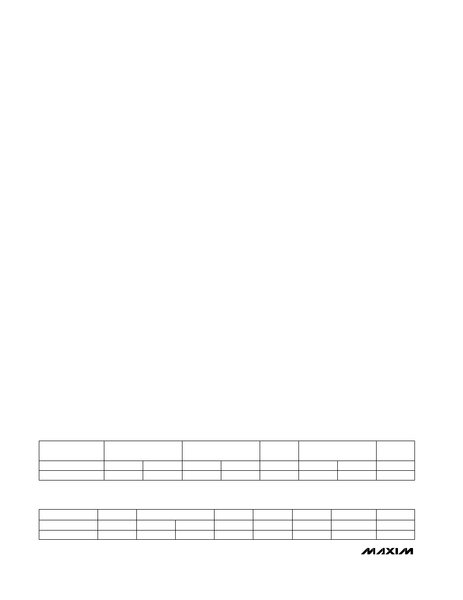
Global Setup Register 1
A1, A0:
(Default = 0, 0) Channel-Selection Control Bits.
These bits (combined with the state of the DIFF, M1,
and M0 bits) determine the channel selected for con-
version according to Tables 8, 9, and 10. These bits
are ignored if the SCAN bit is set.
MF1, MF0:
(Default = 0, 0) Modulator Frequency Bits.
MF1 and MF0 determine the ratio of CLKIN oscillator fre-
quency to modulator operating frequency. They affect
the output data rate, the position of the digital filter notch
frequencies, and the power dissipation of the device.
Achieve lowest power dissipation with MF1 = 0 and MF0
= 0. Highest power dissipation and fastest output data
rate occur with these bits set to 1, 1 (Table 2).
CLK:
(Default = 1) CLK Bit. The CLK bit is used in con-
junction with X2CLK to tell the MAX1401 the frequency
of the CLKIN input signal. If CLK = 0, a CLKIN input fre-
quency of 1.024MHz (2.048MHz for X2CLK = 1) is
expected. If CLK = 1, a CLKIN input frequency of
2.4576MHz (4.9152MHz for X2CLK = 1) is expected.
This bit affects the decimation factor in the digital filter
and thus the output data rate (Table 2).
FS1, FS0:
(Default = 0, 1) Filter Selection Bits. These
bits (in conjunction with the CLK bit) control the deci-
mation ratio of the digital filter. They determine the out-
put data rate, the position of the digital filter frequency
response notches, and the noise present in the output
result (Table 2).
FAST:
(Default 0) Fast Bit. FAST = 0 causes the digital
filter to perform a SINC
3
filter function on the modulator
data stream. The output data rate will be determined by
the values in the CLK, FS1, FS0, MF1, and MF0 bits
(Table 2). The settling time for SINC
3
function is 3
·
[1 /
(output data rate)]. In SINC
3
mode, the MAX1401 auto-
matically holds the DRDY signal false (after any signifi-
cant configuration change) until settled data is
available. FAST = 1 causes the digital filter to perform a
SINC
1
filter function on the modulator data stream. The
signal-to-noise ratio achieved with this filter function is
less than that of the SINC
3
filter; however, SINC
1
settles
in a single output sample period rather than a minimum
of three output sample periods for SINC
3
. When switch-
ing from SINC
1
to SINC
3
mode, the DRDY flag will be
deasserted and reasserted after the filter has fully set-
tled. This mode change requires a minimum of three
samples.
Global Setup Register 2
SCAN:
(Default = 0) Scan Bit. Setting this bit to a 1
causes sequential scanning of the input channels as
determined by DIFF, M1, and M0 (see
Scanning
(
SCAN
Mode
) section). When SCAN = 0, the MAX1401 repeat-
edly measures the unique channel selected by A1, A0,
DIFF, M1, and M0 (Table 4).
M1, M0:
(Default 0, 0) Mode Control Bits. These bits
control access to the calibration channels CALOFF and
CALGAIN. When SCAN = 0, setting M1 = 0 and M0 = 1
selects the CALOFF input, and M1 = 1 and M0 = 0
selects the CALGAIN input (Table 3). When SCAN = 1
and M1
≠
M0, the scanning sequence includes both
CALOFF and CALGAIN inputs (Table 4). When SCAN is
set to 1 and the device is scanning the available input
First Bit (MSB)
(LSB)
First Bit (MSB)
(LSB)
Global Setup Register 2
Global Setup Register 1
FUNCTION
1
FILTER SELECTION
FS0
0
FS1
0
Name
FAST
0
MODULATOR
FREQUENCY
MF0
0
MF1
0
CHANNEL SELECTION
Defaults
A0
1
0
CLK
A1
FUNCTION
0
RESERVED
0
BOUT
0
Name
X2CLK
0
MODE CONTROL
BUFF
0
M0
0
Defaults
M1
0
0
DIFF
SCAN
