Pin description – Rainbow Electronics MAX1401 User Manual
Page 11
MAX1401
+3V, 18-Bit, Low-Power, Multichannel,
Oversampling (Sigma-Delta) ADC
______________________________________________________________________________________
11
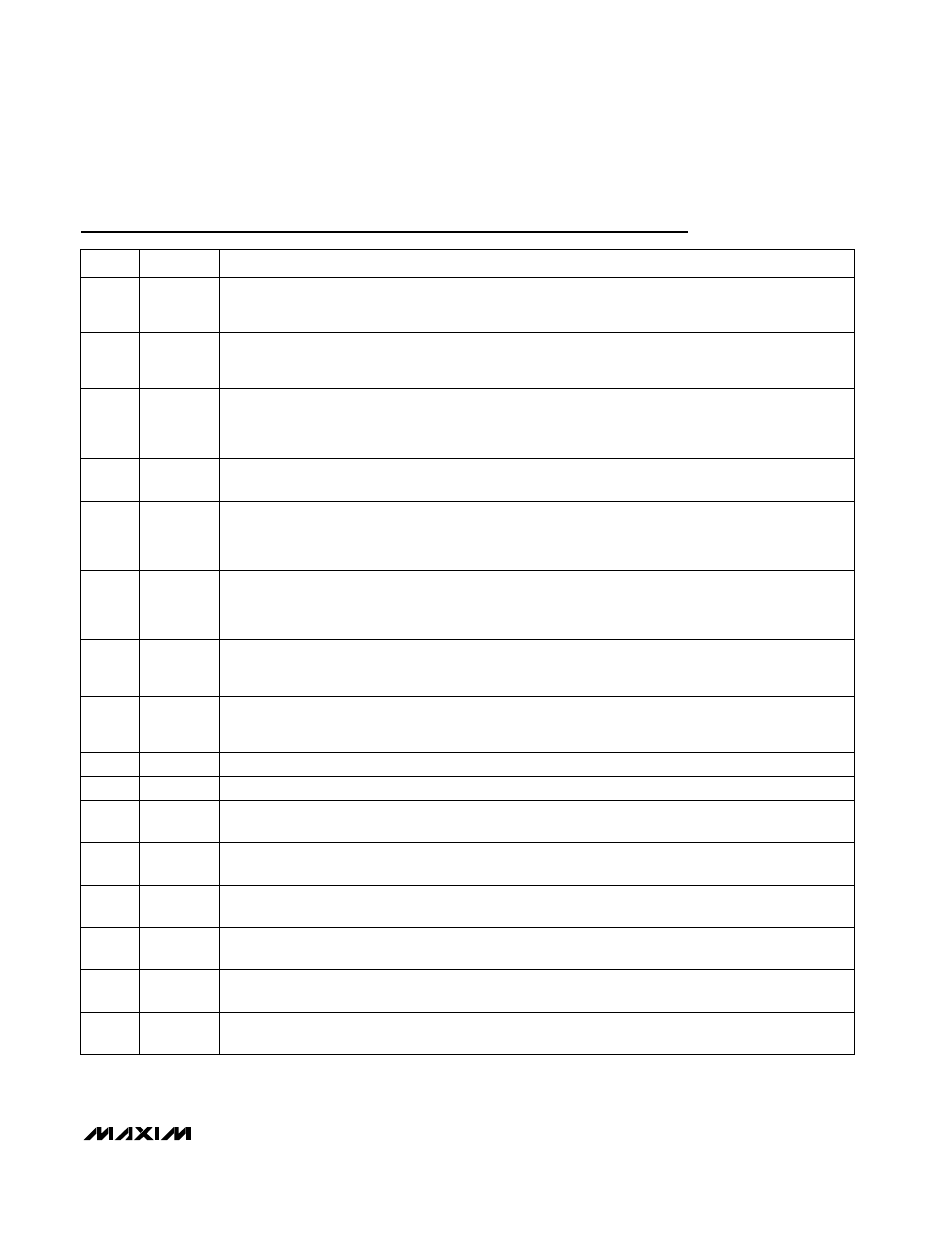
Pin Description
Analog Input 6. May be used as a common point for AIN1 through AIN5 in pseudo-differential mode, or as
the negative input of the AIN5/AIN6 differential analog input pair (see
On-Chip Registers
section).
AIN6
16
Analog Input Channel 4. May be used as a pseudo-differential input with AIN6 as common, or as the neg-
ative input of the AIN3/AIN4 differential analog input pair (see
On-Chip Registers
section).
AIN4
14
Analog Input Channel 3. May be used as a pseudo-differential input with AIN6 as common, or as the posi-
tive input of the AIN3/AIN4 differential analog input pair (see
On-Chip Registers
section).
AIN3
13
Analog Input Channel 2. May be used as a pseudo-differential input with AIN6 as common, or as the neg-
ative input of the AIN1/AIN2 differential analog input pair (see
On-Chip Registers
section).
AIN2
12
Analog Input Channel 1. May be used as a pseudo-differential input with AIN6 as common, or as the posi-
tive input of the AIN1/AIN2 differential analog input pair (see
On-Chip Registers
section).
AIN1
11
Analog Positive Supply Voltage (+2.7V to +3.6V)
V+
10
Analog Ground. Reference point for the analog circuitry. AGND connects to the IC substrate.
AGND
9
Negative Analog Input. A direct input to the negative buffer and the negative differential input terminal of
the ADC - bypassing the input mux. This signal forms a differential input pair with ADCIN+. Connect
ADCIN- to MUXOUT- when direct access is not required.
ADCIN-
8
Positive Analog Input. A direct input to the positive buffer and the positive differential input terminal of the
ADC, bypassing the input mux. This signal forms a differential input pair with ADCIN-. Connect ADCIN+ to
MUXOUT+ when direct access is not required.
ADCIN+
7
Negative Analog Mux Output. The negative differential output signal from the part’s internal input multi-
plexer. Use this signal in conjunction with MUXOUT+ and a high-quality external amplifier for additional
signal processing before conversion. Return the processed output through ADCIN+ and ADCIN-.
Connect MUXOUT- directly to ADCIN- if external processing is not required.
MUXOUT-
6
Positive Analog Mux Output. The positive differential output signal from the part’s internal input multiplex-
er. Use this signal in conjunction with MUXOUT- and a high-quality external amplifier for additional signal
processing before conversion. Return the processed output through ADCIN+ and ADCIN-. Connect
MUXOUT+ directly to ADCIN+ if external processing is not required.
MUXOUT+
5
Active-Low Reset Input. Drive low to reset the control logic, interface logic, digital filter, and analog modu-
lator to power-on status. RESET must be high and CLKIN must be toggling in order to exit reset.
RESET
4
Chip-Select Input. This active-low logic input is used to enable the digital interface. With CS hard-wired
low, the MAX1401 operates in its 3-wire interface mode with SCLK, DIN, and DOUT used to interface to
the device. CS is used either to select the device in systems with more than one device on the serial bus,
or as a frame-synchronization signal for the MAX1401 when a continuous SCLK is used.
CS
3
Clock Output. When deriving the master clock from a crystal, connect the crystal between CLKIN and
CLKOUT. In this mode, the on-chip clock signal is not available at CLKOUT. Leave CLKOUT unconnected
when CLKIN is driven with an external clock.
CLKOUT
2
PIN
Clock Input. A crystal can be connected across CLKIN and CLKOUT. Alternatively, drive CLKIN with a
CMOS-compatible clock at a nominal frequency of 2.4576MHz or 1.024MHz, and leave CLKOUT uncon-
nected. Frequencies of 4.9152MHz and 2.048MHz may be used if the X2CLK control bit is set to 1.
CLKIN
1
FUNCTION
NAME
Analog Input Channel 5. Used as a differential or pseudo-differential input with AIN6 (see
On-Chip
Registers
section).
AIN5
15