Typical operating characteristics (continued), Pin description – Rainbow Electronics MAX1718 User Manual
Page 9
MAX1718
Notebook CPU Step-Down Controller for Intel
Mobile Voltage Positioning (IMVP-II)
_______________________________________________________________________________________
9
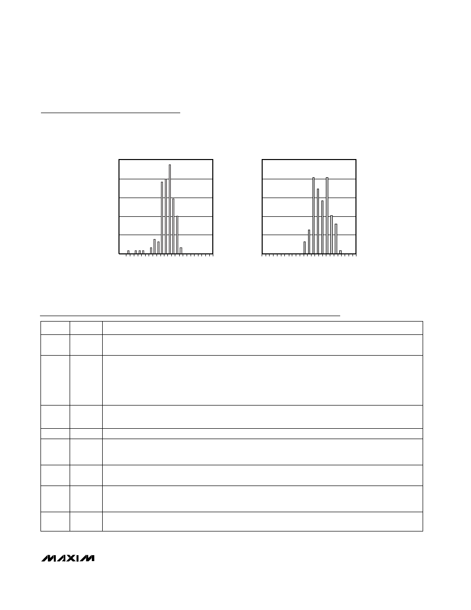
Typical Operating Characteristics (continued)
(Circuit of Figure 1, V+ = 12V, V
DD
= V
CC
= SKP/SDN = 5V, V
OUT
= 1.25V, T
A
= +25°C, unless otherwise noted.)
0
5
15
10
20
25
-0.48
OUTPUT VOLTAGE DISTRIBUTION
MAX1718 toc17
OUTPUT VOLTAGE ERROR (%)
SAMPLE PERCENTAGE (%)
-0.24
0.48
0.24
0.00
V
OUT
= 1.25V
0
5
15
10
20
25
1.995
REFERENCE VOLTAGE DISTRIBUTION
MAX1718 toc18
REFERENCE VOLTAGE (V)
SAMPLE PERCENTAGE (%)
1.998
2.005
2.002
2.000
Analog Supply Voltage Input for PWM Core. Connect V
CC
to the system supply voltage (4.5V to 5.5V) with a
series 20
Ω resistor. Bypass to GND with a 0.22µF (min) capacitor.
V
CC
9
Suspend-Mode Voltage Select Input. S0 and S1 are four-level digital inputs that select the suspend-mode
VID code for the suspend-mode multiplexer inputs. If SUS is high, the suspend-mode VID code is delivered
to the DAC (see the Internal Multiplexers (ZMODE/SUS) section).
S0, S1
7, 8
6
CC
Integrator Capacitor Connection. Connect a 47pF to 1000pF (47pF typ) capacitor from CC to GND to set the
integration time constant (see the Integrator Amplifiers/Output Voltage Offsets section).
Feedback Offset Adjust Negative Input. The output shifts by an amount equal to the difference between POS
and NEG multiplied by a scale factor that depends on the DAC codes (see the Integrator Amplifiers/Output
Voltage Offsets section). Connect both POS and NEG to REF if the offset function is not used.
NEG
5
4
FB
Feedback Input. Connect FB to the junction of the external inductor and the positioning resistor (Figure 1).
Slew-Rate Adjustment Pin. Connect a resistor from TIME to GND to set the internal slew-rate clock. A 470k
Ω
to 47k
Ω resistor sets the clock from 38kHz to 380kHz, f
SLEW
= 150kHz
✕
120k
Ω / R
TIME
.
TIME
3
2
SKP/SDN
Combined Shutdown and Skip-Mode Control. Drive SKP/SDN to GND for shutdown. Leave SKP/SDN open for
low-noise forced-PWM mode, or drive to V
CC
for pulse-skipping operation. Low-noise forced-PWM mode caus-
es inductor current recirculation at light loads and suppresses pulse-skipping operation. Forcing SKP/SDN to
12V to 15V disables both the overvoltage protection and undervoltage protection circuits and clears the fault
latch, with otherwise normal pulse-skipping operation. Do not connect SKP/SDN to > 15V.
Battery Voltage Sense Connection. Connect V+ to input power source. V+ is used only for PWM one-shot
timing. DH on-time is inversely proportional to input voltage over a range of 2V to 28V.
V+
1
PIN
NAME
FUNCTION
Pin Description