Rainbow Electronics MAX1718 User Manual
Page 15
MAX1718
Notebook CPU Step-Down Controller for Intel
Mobile Voltage Positioning (IMVP-II)
______________________________________________________________________________________
15
Thus, it is necessary to use forced PWM mode during all
negative transitions. Most applications should use PWM
mode exclusively, although there is some benefit to
using skip mode while in the low-power suspend state
(see the Using Skip Mode During Suspend (SKP/
SDN
=
V
CC
) section.)
Automatic Pulse-Skipping Switchover
In skip mode (SKP/SDN high), an inherent automatic
switchover to PFM takes place at light loads (Figure 6).
This switchover is effected by a comparator that trun-
cates the low-side switch on-time at the inductor current’s
zero crossing. This mechanism causes the threshold
between pulse-skipping PFM and nonskipping PWM
operation to coincide with the boundary between con-
tinuous and discontinuous inductor-current operation.
The load-current level at which PFM/PWM crossover
occurs, I
LOAD(SKIP)
, is equal to 1/2 the peak-to-peak
ripple current, which is a function of the inductor value
(Figure 6). For a battery range of 7V to 24V, this thresh-
old is relatively constant, with only a minor dependence
on battery voltage:
where K is the on-time scale factor (Table 2). For exam-
ple, in the standard application circuit this becomes:
The crossover point occurs at a lower value if a swing-
ing (soft-saturation) inductor is used.
The switching waveforms may appear noisy and asyn-
chronous when light loading causes pulse-skipping
operation, but this is a normal operating condition that
results in high light-load efficiency. Trade-offs in PFM
noise vs. light-load efficiency are made by varying the
inductor value. Generally, low inductor values produce
a broader efficiency vs. load curve, while higher values
result in higher full-load efficiency (assuming that the
coil resistance remains fixed) and less output voltage
ripple. Penalties for using higher inductor values
include larger physical size and degraded load-tran-
sient response, especially at low input voltage levels.
Current-Limit Circuit
The current-limit circuit employs a unique “valley” current-
sensing algorithm that uses the on-resistance of the
low-side MOSFET as a current-sensing element. If the
current-sense signal is above the current-limit thresh-
old, the PWM is not allowed to initiate a new cycle
3 3
1 25
2
0 68
12
1 25
12
2 7
.
.
.
.
.
µ
µ
s
V
H
V
V
V
A
Ч
Ч
Ч
−
=
I
K
V
L
V
V
V
LOAD SKIP
OUT
BATT
OUT
BATT
(
)
≈
Ч
Ч
Ч
−
2
REF
MAX1718
POS
NEG
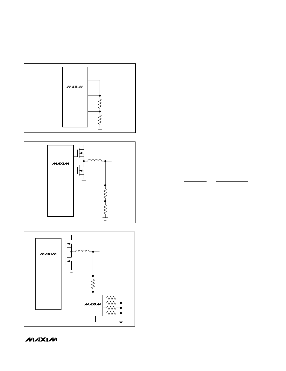
Figure 3. Resistive Divider from REF
DL
DH
MAX1718
POS
NEG
Figure 4. Resistive Divider from OUTPUT
DL
DH
B
A
MAX1718
SEL
MUX
POS
NEG
MAX4524
Figure 5. Programmable Offset Voltage