Table 2. approximate k-factor errors – Rainbow Electronics MAX1718 User Manual
Page 14
MAX1718
Notebook CPU Step-Down Controller for Intel
Mobile Voltage Positioning (IMVP-II)
14
______________________________________________________________________________________
external high-side MOSFET. Resistive losses, including
the inductor, both MOSFETs, output capacitor ESR, and
PC board copper losses in the output and ground tend
to raise the switching frequency at higher output cur-
rents. Also, the dead-time effect increases the effective
on-time, reducing the switching frequency. It occurs
only in PWM mode (SKP/SDN = open) and during
dynamic output voltage transitions when the inductor
current reverses at light or negative load currents. With
reversed inductor current, the inductor’s EMF causes
LX to go high earlier than normal, extending the on-time
by a period equal to the DH-rising dead time.
For loads above the critical conduction point, where the
dead-time effect is no longer a factor, the actual switching
frequency is:
where V
DROP1
is the sum of the parasitic voltage drops
in the inductor discharge path, including synchronous
rectifier, inductor, and PC board resistances; V
DROP2
is
the sum of the parasitic voltage drops in the inductor
charge path, including high-side switch, inductor, and
PC board resistances; and t
ON
is the on-time calculat-
ed by the MAX1718.
Integrator Amplifiers/Output
Voltage Offsets
Two transconductance integrator amplifiers provide a
fine adjustment to the output regulation point. One
amplifier forces the DC average of the feedback volt-
age to equal the VID DAC setting. The second amplifier
is used to create small positive or negative offsets from
the VID DAC setting, using the POS and NEG pins.
The integrator block has the ability to lower the output
voltage by 8% and raise it by 8%. For each amplifier,
the differential input voltage range is at least ±80mV
total, including DC offset and AC ripple. The two ampli-
fiers’ outputs are directly summed inside the chip, so
the integration time constant can be set easily with one
capacitor at the CC pin. Use a capacitor value of 47pF
to 1000pF (47pF typ). The g
m
of each amplifier is
160µmho (typ).
The POS/NEG amplifier is used to add small offsets to
the VID DAC setting or to correct for voltage drops. To
create an output offset, bias POS and NEG to a voltage
(typically V
OUT
or REF) within their common-mode
range, and offset them from one another with a resistive
divider (Figures 3 and 4). If V
POS
is higher than V
NEG
,
then the output is shifted in the positive direction. If
V
NEG
is higher than V
POS
, then the output is shifted in
the negative direction. The amount of output offset is
less than the difference from POS to NEG by a scale
factor that varies with the VID DAC setting as shown in
Table 3. The common-mode range of POS and NEG is
0.4V to 2.5V.
For applications that require multiple offsets, an exter-
nal multiplexer can be used to select various resistor
values (Figure 5).
Both the integrator amplifiers can be disabled by con-
necting NEG to V
CC
.
Forced-PWM Mode (SKP/
SDN
Open)
The low-noise forced-PWM mode (SKP/SDN open) dis-
ables the zero-crossing comparator, allowing the induc-
tor current to reverse at light loads. This causes the
low-side gate-drive waveform to become the comple-
ment of the high-side gate-drive waveform. The benefit
of forced-PWM mode is to keep the switching frequen-
cy fairly constant, but it comes at a cost: the no-load
battery current can be 10mA to 40mA, depending on
the external MOSFETs and switching frequency.
Forced-PWM mode is required during downward output
voltage transitions. The MAX1718 uses PWM mode dur-
ing all transitions, but only while the slew-rate controller
is active. Due to voltage positioning, when a transition
uses high negative inductor current, the output voltage
does not settle to its final intended value until well after
the slew-rate controller terminates. Because of this it is
possible, at very high negative slew currents, for the out-
put to end up high enough to cause VGATE to go low.
f
V
V
t
V
V
V
OUT
DROP
ON
IN
DROP
DROP
=
+
+
−
(
)
(
)
1
1
2
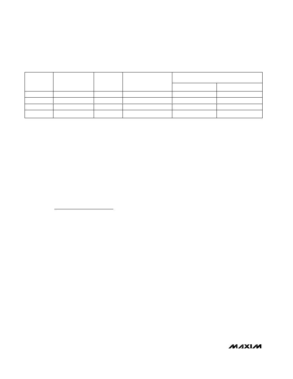
Table 2. Approximate K-Factor Errors
MIN RECOMMENDED V
BATT
AT
TON
SETTING
TON
FREQUENCY
(kHZ)
K-FACTOR
(µs)
APPROXIMATE K-
FACTOR ERROR (%)
V
OUT
= 1.25V (V)
V
OUT
= 1.75V (V)
V
CC
200
5
±10
1.7
2.3
OPEN
300
3.3
±10
1.8
2.5
REF
550
1.8
±12.5
2.6
3.5
GND
1000
1.0
±12.5
3.6
4.9