Electrical characteristics (continued) – Rainbow Electronics MAX1403 User Manual
Page 6
MAX1403
+3V, 18-Bit, Low-Power, Multichannel,
Oversampling (Sigma-Delta) ADC
6
_______________________________________________________________________________________
Note 1:
Contact factory for INL limits applicable with FS1 = 0 and MF1, MF0 = 1, 2, or 3.
Note 2:
Nominal gain is 0.98. This ensures a full-scale input voltage may be applied to the part under all conditions without caus-
ing saturation of the digital output data.
Note 3:
Positive Full-Scale Error includes zero-scale errors (unipolar offset error or bipolar zero error) and applies to both unipolar
and bipolar input ranges. This error does not include the nominal gain of 0.98.
Note 4:
Full-Scale Drift includes zero-scale drift (unipolar offset drift or bipolar zero drift) and applies to both unipolar and bipolar
input ranges.
Note 5:
Gain Error does not include zero-scale errors. It is calculated as (full-scale error - unipolar offset error) for unipolar ranges
and as (full-scale error - bipolar zero error) for bipolar ranges. This error does not include the nominal gain of 0.98.
Note 6:
Gain-Error Drift does not include unipolar offset drift or bipolar zero drift. It is effectively the drift of the part if zero-scale
error is removed.
Note 7:
Use of the offset DAC does not imply that any input may be taken below AGND.
Note 8:
Additional noise added by the offset DAC is dependent on the filter cutoff, gain, and DAC setting. No noise is added for a
DAC code of 0000.
Note 9:
Guaranteed by design or characterization; not production tested.
Note 10:
The absolute input voltage must be within the input voltage range specification.
Note 11:
All AIN and REFIN pins have identical input structures. Leakage is production tested only for the AIN3, AIN4, AIN5,
CALGAIN, and CALOFF inputs.
Note 12:
The dynamic load presented by the MAX1403 analog inputs for each gain setting is discussed in detail in the
Switching
Network
section
.
Values are provided for the maximum allowable external series resistance.
Note 13:
The input voltage range for the analog inputs is with respect to the voltage on the negative input of its respective differen-
tial or pseudo-differential pair. Table 5 shows which inputs form differential pairs.
Note 14:
V
REF
= V
REFIN+
- V
REFIN-
.
Note 15:
These specifications apply to CLKOUT only when driving a single CMOS load.
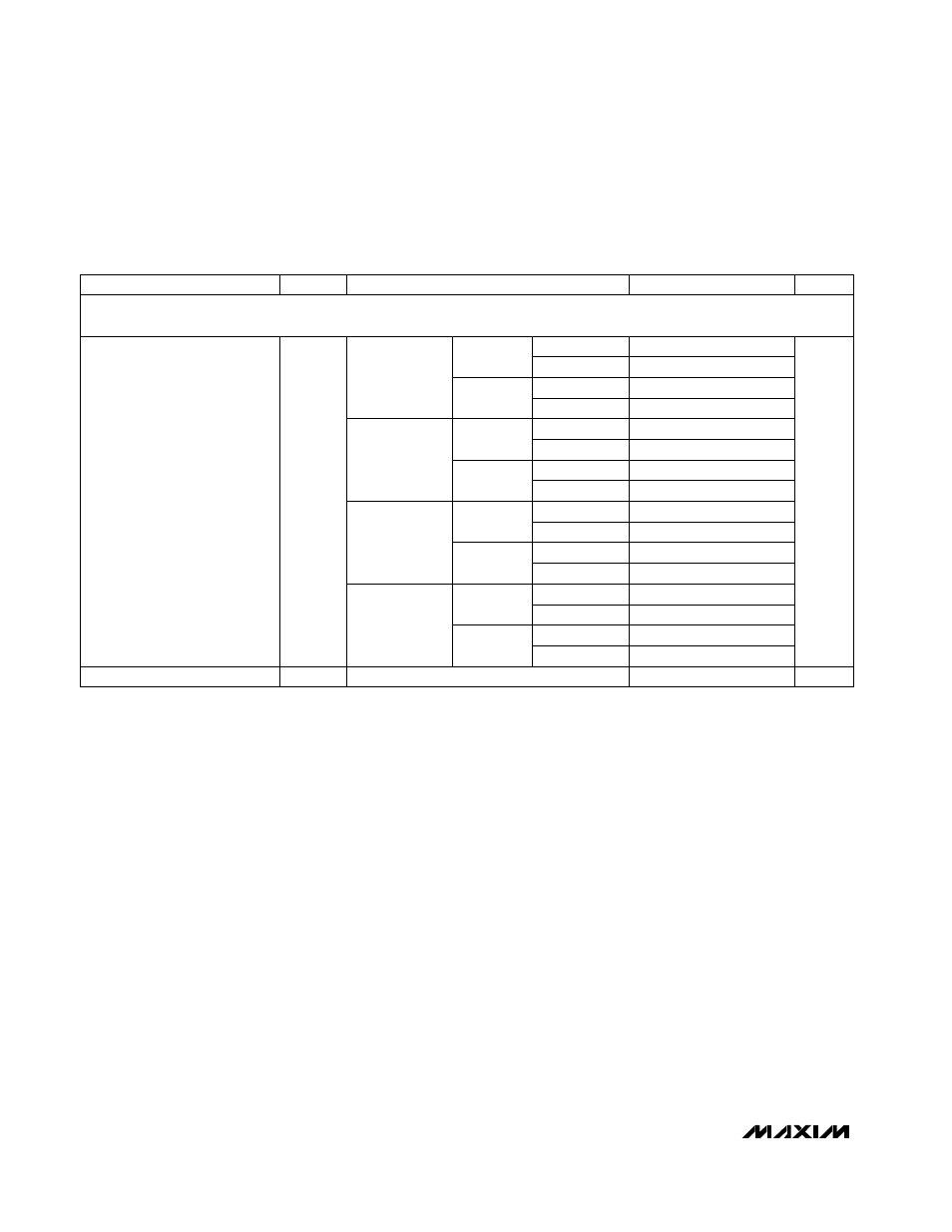
2.4576MHz
1.024MHz
Buffers off
Buffers off
Buffers on
2.4576MHz
1.024MHz
1.45
2.05
Buffers off
Buffers off
Buffers on
Normal mode,
MF1 = 0,
MF0 = 0
2.51
3.30
1.32
1.98
Buffers on
2.28
Buffers on
2X mode,
MF1 = 0,
MF0 = 1
4.53
6.11
CONDITIONS
1.95
2.97
1.08
2.4576MHz
1.024MHz
Buffers off
Buffers off
Buffers on
2.4576MHz
1.024MHz
4.32
Buffers off
Buffers off
Buffers on
4X mode,
MF1 = 1,
MF0 = 0
16.6
21.2
6.67
8.58
Buffers on
16.4
Buffers on
8X mode,
MF1 = 1,
MF0 = 1
mW
16.9
21.45
PD
Power Dissipation
7.0
8.91
6.44
1.75
(Note 19)
7
70
µW
Standby Power Dissipation
0.81
1.36
UNITS
MIN
TYP
MAX
SYMBOL
PARAMETER
ELECTRICAL CHARACTERISTICS (continued)
(V+ = +2.7V to +3.6V, V
DD
= +2.7V to +3.6V, V
REFIN+
= +1.25V, REFIN- = AGND, f
CLKIN
= 2.4576MHz, T
A
= T
MIN
to T
MAX
, unless
otherwise noted. Typical values are at T
A
= +25°C.)
POWER DISSIPATION
(V+ = V
DD
= +3.3V, digital inputs = 0 or V
DD
, external CLKIN, burn-out and transducer excitation currents
disabled, X2CLK = 0, CLK = 0 for 1.024MHz, CLK = 1 for 2.4576MHz.)