Detailed description, Circuit description – Rainbow Electronics MAX1403 User Manual
Page 13
MAX1403
+3V, 18-Bit, Low-Power, Multichannel,
Oversampling (Sigma-Delta) ADC
______________________________________________________________________________________
13
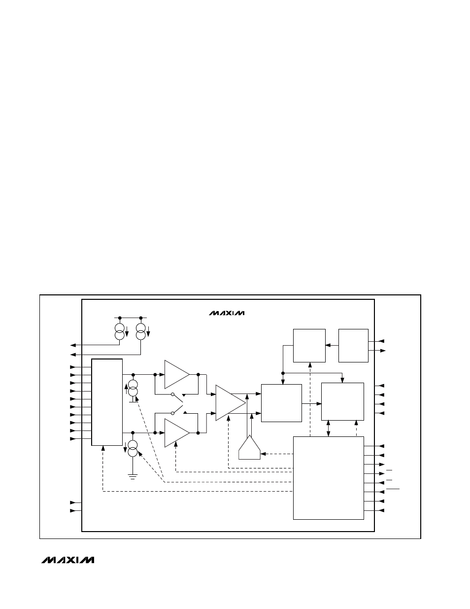
_______________Detailed Description
Circuit Description
The MAX1403 is a low-power, multichannel, serial-output,
sigma-delta ADC designed for applications with a wide
dynamic range, such as weigh scales and pressure
transducers. The functional block diagram in Figure 2
contains a switching network, a modulator, a PGA, two
buffers, an oscillator, an on-chip digital filter, two
matched transducer excitation current sources, and a
bidirectional serial communications port.
Three fully differential input channels feed into the
switching network. Each channel may be independent-
ly programmed with a gain between +1V/V and
+128V/V. These three differential channels may also be
configured to operate as five pseudo-differential input
channels. Two additional, fully differential system-cali-
bration channels allow system gain and offset error to
be measured. These system-calibration channels can
be used as additional differential signal channels when
dedicated gain and offset error correction channels are
not required.
Two chopper-stabilized buffers are available to isolate
the selected inputs from the capacitive loading of the
PGA and modulator. Three independent DACs provide
compensation for the DC component of the input signal
on each of the differential input channels.
The sigma-delta modulator converts the input signal into
a digital pulse train whose average duty cycle represents
the digitized signal information. The pulse train is then
processed by a digital decimation filter, resulting in a
conversion accuracy exceeding 16 bits. The digital filter’s
decimation factor is user-selectable, which allows the
conversion result’s resolution to be reduced to achieve a
higher output data rate. When used with 2.4576MHz or
1.024MHz master clocks, the decimation filter can be
programmed to produce zeros in its frequency response
at the line frequency and associated harmonics. This
ensures excellent line rejection without the need for fur-
ther postfiltering. In addition, the modulator sampling
frequency can be optimized for either lowest power dis-
sipation or highest output data rate.
AGND
V+
DGND
V
DD
CALOFF+
OUT2
OUT1
CALGAIN+
CALOFF-
CALGAIN-
AIN1
AIN2
AIN3
AIN4
AIN5
AIN6
SWITCHING
NETWORK
MODULATOR
DAC
PGA
V+
BUFFER
BUFFER
AGND
V+
DIGITAL
FILTER
SCLK
DIN
DOUT
INT
CS
DS0
DS1
RESET
CLKIN
CLKOUT
REFIN+
REFIN-
DIVIDER
MAX1403
INTERFACE
AND CONTROL
CLOCK
GEN
Figure 2. Functional Diagram