Offset-correction dac, Clock oscillator – Rainbow Electronics MAX1403 User Manual
Page 28
MAX1403
+3V, 18-Bit, Low-Power, Multichannel,
Oversampling (Sigma-Delta) ADC
28
______________________________________________________________________________________
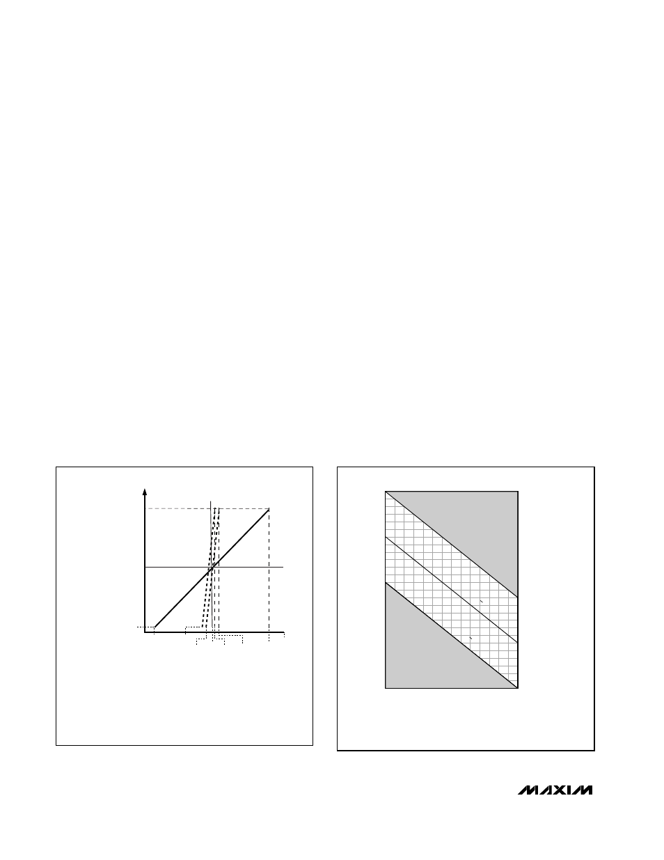
Offset-Correction DAC
The MAX1403 provides a coarse (3-bit plus sign) offset-
correction DAC at the modulator input. Use this DAC to
remove the offset component in the input signal, allow-
ing the ADC to operate on a more sensitive range. The
DAC offsets up to ±116.7% of the selected range in
±16.7% increments for unipolar mode, and up to
±58.3% of the selected range in ±8.3% increments for
bipolar mode. When a DAC value of 0 is selected, the
DAC is completely disconnected from the modulator
inputs and does not contribute any noise. Figures 8
and 9 show the effect of the DAC codes on the input
range and transfer function.
Clock Oscillator
The clock oscillator may be used with an external crystal
(or resonator) connected between CLKIN and CLKOUT,
or may be driven directly by an external oscillator at
CLKIN with CLKOUT left unconnected. In normal oper-
ating mode, the MAX1403 is specified for operation with
CLKIN at either 1.024MHz (CLK = 0) or 2.4576MHz
(CLK = 1, default). When operated at these frequencies,
the device may be programmed to produce frequency
response nulls at the local line frequency (either 60Hz or
50Hz) and the associated line harmonics.
In standby mode (STBY = 1) all circuitry, with the
exception of the serial interface and the clock oscillator,
is powered down. The interface consumes minimal
power with a static SCLK. Enter power-down mode
(including the oscillator) by setting the FULLPD bit in
the special-function register. When exiting a full-power
shutdown, perform a hardware reset or a software reset
after the master clock signal is established (typically
10ms when using the on-board oscillator with an exter-
nal crystal) to ensure that any potentially corrupted reg-
isters are cleared.
It is often helpful to use higher-frequency crystals or
resonators, especially for surface-mount applications
where the result may be reduced PC board area for the
oscillator component and a lower price or better com-
ponent availability. Also, it may be necessary to oper-
ate the part with a clock source whose duty cycle is not
close to 50%. In either case, the MAX1403 can operate
with a master clock frequency of up to 5MHz, and
includes an internal divide-by-2 prescaler to restore the
internal clock frequency to a range of up to 2.5MHz
with a 50% duty cycle. To activate this prescaler, set
the X2CLK bit in the control registers. Note that using
CLKIN frequencies above 2.5MHz in combination with
the X2CLK mode will result in a small increase in digital
supply current.
DAC CODE
D3:
D2:
D1:
D0:
INPUT VOLTAGE RANGE
(V
REF
= 1.25V
PGA = 000)
-7
1
1
1
1
-6
1
1
1
0
-5
1
1
0
1
-4
1
1
0
0
-3
1
0
1
1
-2
1
0
1
0
-1
1
0
1
0
0
0
0
0
0
+1
0
0
0
1
+2
0
0
1
0
+3
0
0
1
1
+4
0
1
0
0
+5
0
1
0
1
+6
0
1
1
0
+7
0
1
1
1
2.708V
2.50V
2.292V
2.083V
1.875V
1.667V
1.458V
1.25V
1.042V
0.833V
0.625V
0.416V
0.208V
0V
-0.208V
-0.416V
-0.625V
-0.833V
-1.042V
-1.25V
-1.458V
-1.667V
-1.875V
-2.083V
-2.292V
-2.50V
-2.708V
13/6 V
REF
/2
PGA
2 V
REF
/2
PGA
11/6 V
REF
/2
PGA
10/6 V
REF
/2
PGA
9/6 V
REF
/2
PGA
8/6 V
REF
/2
PGA
7/6 V
REF
/2
PGA
V
REF
/2
PGA
5/6 V
REF
/2
PGA
4/6 V
REF
/2
PGA
3/6 V
REF
/2
PGA
2/6 V
REF
/2
PGA
1/6 V
REF
/2
PGA
0
-1/6 V
REF
/2
PGA
-2/6 V
REF
/2
PGA
-3/6 V
REF
/2
PGA
-4/6 V
REF
/2
PGA
-5/6 V
REF
/2
PGA
-V
REF
/2
PGA
-7/6 V
REF
/2
PGA
-8/6 V
REF
/2
PGA
-9/6 V
REF
/2
PGA
-10/6 V
REF
/2
PGA
-11/6 V
REF
/2
PGA
-2 V
REF
/2
PGA
-13/6 V
REF
/2
PGA
MAXIMUM INPUT
MINIMUM INPUT (U/B = 1)
MINIMUM INPUT (U/B = 0)
Figure 9. Input Voltage Range vs. DAC Code
ZERO-SCALE 2621
MIDSCALE 131072
NEGATIVE DAC STEP
SHIFTS THE TRANSFER
FUNCTION TOWARD
THE POSITIVE RAIL.
PGA = 3
DAC = 0
PGA = 0
DAC = 0
PGA = 3
DAC = +3
MAX CODE 262144
FULL-SCALE 259522
INPUT VOLTAGE RANGE
CODE
(V
AIN
-)-V
REF
AGND
(V
AIN
-) - V
REF
/8 - V
REF
/16
(V
AIN
-) - V
REF
/8 - V
REF
/16
(V
AIN
-) - V
REF
/8
(V
AIN
-) + V
REF
/8
V+
(V
AIN
-) + V
REF
(V
AIN-
)
Figure 8. Effect of PGA and DAC Codes on the Bipolar Transfer
Function