Table 1. control-register addressing, Serial digital interface, Applications information – Rainbow Electronics MAX1403 User Manual
Page 14: Modulator data output
MAX1403
+3V, 18-Bit, Low-Power, Multichannel,
Oversampling (Sigma-Delta) ADC
14
______________________________________________________________________________________
The MAX1403 can be configured to sequentially scan
all signal inputs and to transmit the results through the
serial interface with minimum communications over-
head. The output word contains a channel identification
tag to indicate the source of each conversion result.
Serial Digital Interface
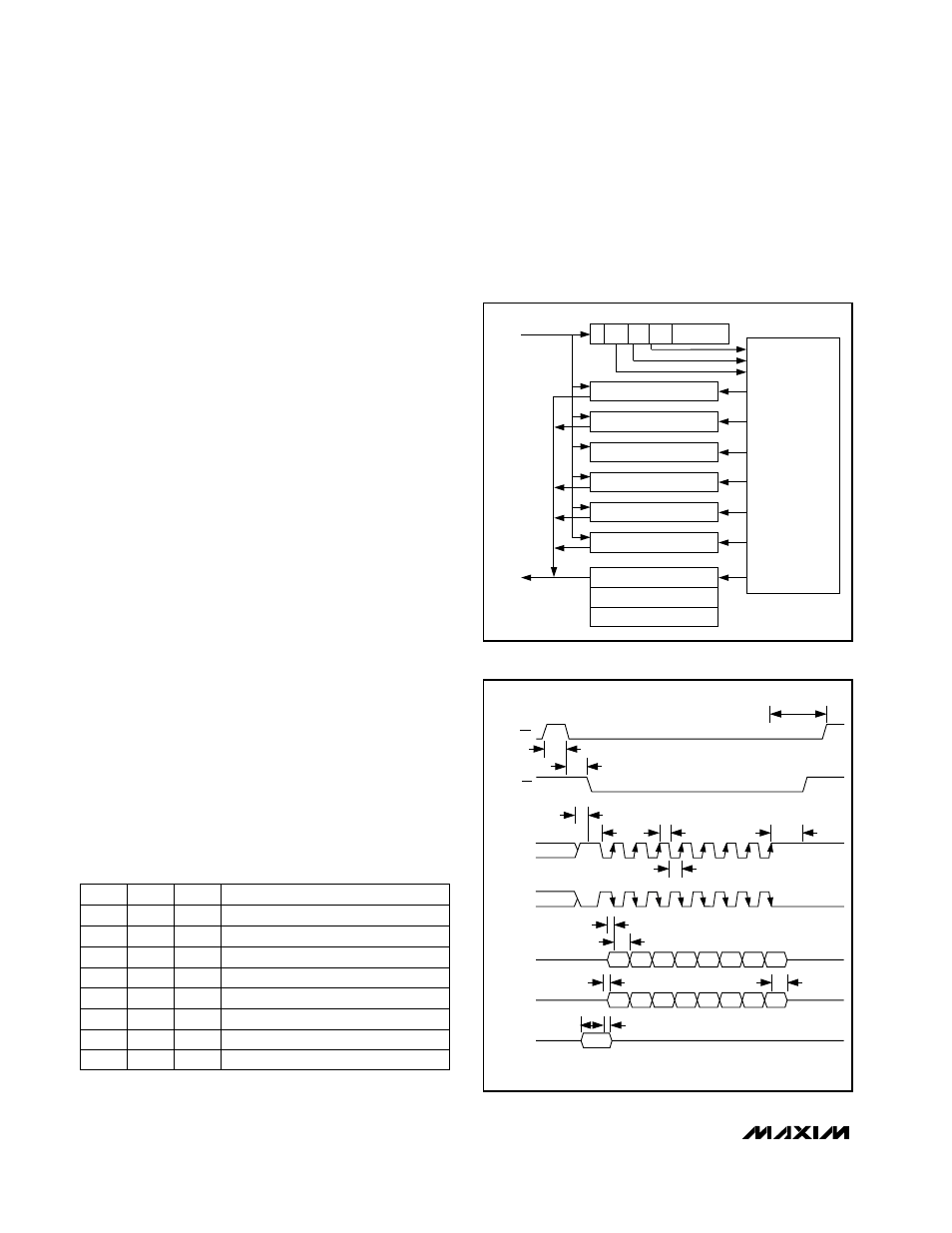
The serial digital interface provides access to eight on-
chip registers (Figure 3). All serial-interface commands
begin with a write to the communications register
(COMM). On power-up, system reset, or interface reset,
the part expects a write to its communications register.
The COMM register access begins with a 0 start bit.
The COMM register R/W bit selects a read or write
operation, and the register select bits (RS2, RS1, RS0)
select the register to be addressed. Hold DIN high
when not writing to COMM or another register (Table 1).
The serial interface consists of five signals: CS, SCLK,
DIN, DOUT, and INT. Clock pulses on SCLK shift bits
into DIN and out of DOUT. INT provides an indication
that data is available. CS is a device chip-select input
as well as a clock polarity select input (Figure 4).
Using CS allows the SCLK, DIN, and DOUT signals to
be shared among several SPI-compatible devices.
When short on I/O pins, connect CS low and operate
the serial digital interface in CPOL = 1, CPHA = 1 mode
using SCLK, DIN, and DOUT. This 3-wire interface mode
is ideal for opto-isolated applications. Furthermore, a
microcontroller (such as a PIC16C54 or 80C51) can
use a single bidirectional I/O pin for both sending to
DIN and receiving from DOUT (see
Applications
Information
), because the MAX1403 drives DOUT only
during a read cycle.
Additionally, connecting the INT signal to a hardware
interrupt allows faster throughput and reliable, collision-
free data flow.
The MAX1403 features a mode where the raw modula-
tor data output is accessible. In this mode, the DOUT
and INT functions are reassigned (see the
Modulator
Data Output
section).
DATA REGISTER D1–D0/CID
RS0
GLOBAL SETUP REGISTER 1
GLOBAL SETUP REGISTER 2
SPECIAL FUNCTION REGISTER
XFER FUNCTION REGISTER 1
XFER FUNCTION REGISTER 2
XFER FUNCTION REGISTER 3
DATA REGISTER D17–D10
DATA REGISTER D9–D2
COMMUNICATIONS REGISTER
RS1
RS2
DIN
DOUT
REGISTER
SELECT
DECODER
Figure 3. Register Summary
DIN
(DURING
WRITE)*
DOUT
(DURING
READ)*
DS1, DS0
MSB D6
D5
D4
D3
D2
D1
D0
MSB D6
D5
D4
D3
D2
D1
D0
CS
INT
t
10
t
6
t
20
t
19
t
8
t
7
t
17
t
16
t
3
t
1
t
13
t
5
t
4
t
12
t
18
t
9
t
11
t
15
t
14
SCLK
(CPOL = 1)
SCLK
(CPOL = 0)
*DOUT
IS HIGH IMPEDANCE DURING THE WRITE CYCLE; DIN IS IGNORED
DURING THE READ CYCLE.
Figure 4. Serial-Interface Timing
Table 1. Control-Register Addressing
0
RS1
0
RS0
0
1
Global Setup Register 1
0
1
0
1
1
Special Function Register
0
Global Setup Register 2
Communications Register
0
0
0
0
0
1
Transfer Function Register 2
1
1
0
1
1
Data Register
1
Transfer Function Register 3
Transfer Function Register 1
1
1
RS2
TARGET REGISTER