Table 11. channel id tag codes, Switching network – Rainbow Electronics MAX1403 User Manual
Page 22
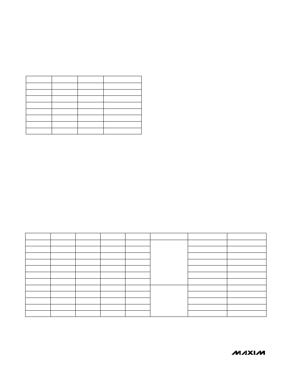
DS1, DS0:
The status of the auxiliary data input pins.
These are latched on the first falling edge of the SCLK
signal for the current data register read access.
CID2–0:
Channel ID tag (Table 11).
Switching Network
A switching network provides selection between three
fully differential input channels or five pseudo-differen-
tial channels, using AIN6 as a shared common. The
switching network provides two additional fully differen-
tial input channels intended for system calibration,
which may be used as extra fully differential signal
channels. Table 12 shows the channel configurations
available for both operating modes.
Scanning (SCAN-Mode)
To sample and convert the available input channels
sequentially, set the SCAN control bit in the global
setup register. The sequence is determined by DIFF
(fully differential or pseudo-differential) and by the
mode control bits M1 and M0 (Tables 8, 9, 10). With
SCAN set, the device automatically sequences through
each available channel, transmitting a single conver-
sion result before proceeding to the next channel. The
MAX1403 automatically allows sufficient time for each
conversion to fully settle, to ensure optimum resolution
before asserting the data-ready signal and moving to
the next available channel. The scan rate is, therefore,
dependent on the clock bit (CLK), the filter control bits
(FS1, FS0), and the modulator frequency selection bits
(MF1, MF0).
Burn-Out Currents
The input circuitry also provides two “burn-out” cur-
rents. These small currents may be used to test the
integrity of the selected transducer. They can be selec-
tively enabled or disabled by the BOUT bit in the global
setup register.
Table 12. Input Channel Configuration in Fully Differential and Pseudo-Differential
Mode (SCAN = 0)
X = Don’t care
*
This combination is available only in pseudo-differential mode when using the internal scanning logic.
**
These combinations are only available in the calibration modes.
0
M0
0
DIFF
0
0
AIN2
0
0
0
0
0
AIN4
0
AIN3
AIN1
0
0
0
1
0
1
AIN3
0
0
1
1
X
CALOFF+**
0
AIN5
AIN1
0
0
0
X
1
X
CALOFF+**
M1
0
0
X
HIGH INPUT
CALGAIN+**
AIN5*
1
0
0
X
CALGAIN+**
1
0
A1
0
1
1
0
0
1
X
X
X
X
X
MODE
Pseudo-
Differential
Fully
Differential
0
A0
1
0
1
0
1
0
X
X
X
X
X
AIN6
AIN6
AIN6
AIN6
AIN4
CALOFF-**
AIN6
AIN2
CALOFF-**
LOW INPUT
CALGAIN-**
AIN6*
CALGAIN-**
Calibration
AIN5–AIN6
AIN3–AIN4
AIN1–AIN2
AIN4–AIN6
AIN3–AIN6
AIN2–AIN6
AIN1–AIN6
CHANNEL
CID0
0
1
0
1
0
1
0
1
1
1
0
0
1
1
0
0
CID1
CID2
0
0
0
0
1
1
1
1
MAX1403
+3V, 18-Bit, Low-Power, Multichannel,
Oversampling (Sigma-Delta) ADC
22
______________________________________________________________________________________
Table 11. Channel ID Tag Codes