Table 13c. r – Rainbow Electronics MAX1403 User Manual
Page 24
MAX1403
+3V, 18-Bit, Low-Power, Multichannel,
Oversampling (Sigma-Delta) ADC
24
______________________________________________________________________________________
Table 13c. R
EXT
, C
EXT
Values for Less than 16-Bit Gain Error in Unbuffered (BUFF = 0)
Mode—4x Modulator Sampling Frequency (MF1, MF0 = 10 ); X2CLK = 0; CLKIN =
2.4576MHz
Table 13d. R
EXT
, C
EXT
Values for Less than 16-Bit Gain Error in Unbuffered (BUFF = 0)
Mode—8x Modulator Sampling Frequency (MF1, MF0 = 11); X2CLK = 0; CLKIN =
2.4576MHz
R
EXT
C
EXT
R
MUX
C
PIN
R
IN
C
ST
C
AMP
C
SAMPLE
C
C
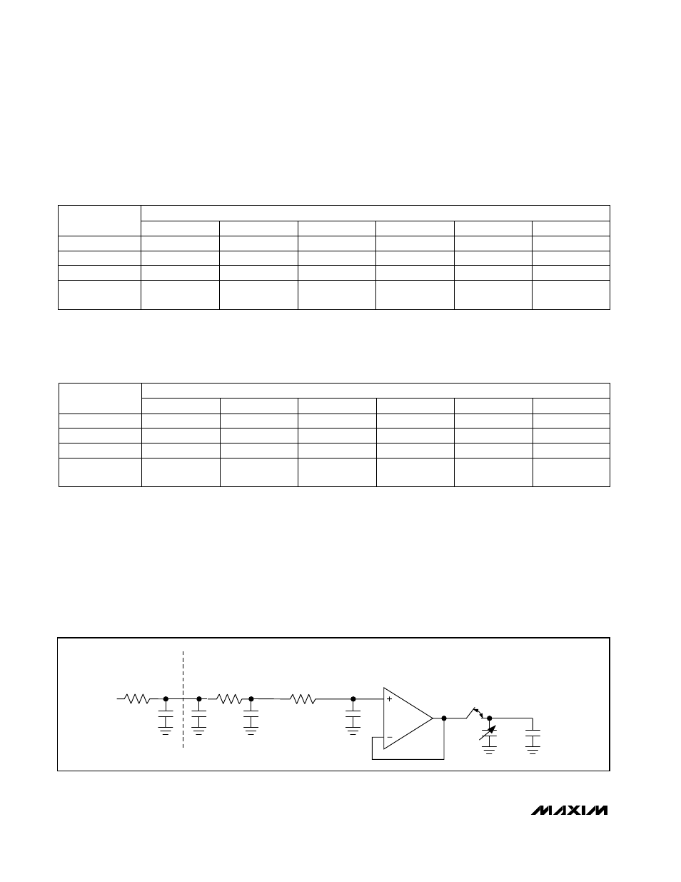
Figure 6
. Analog Input, Buffered Mode (BUFF = 1)
8.3
3.7
8.3
3.7
2.4
2
6.2
3.2
4.1
2.5
1.8
8, 16, 32,
64, 128
2.2
2.4
4
1
C
EXT
= 0pF
C
EXT
= 50pF
C
EXT
= 100pF
0.72
0.40
0.72
0.40
0.11
0.67
0.38
0.60
0.35
0.09
0.10
PGA GAIN
0.11
C
EXT
= 500pF
C
EXT
= 1000pF
C
EXT
= 5000pF
EXTERNAL RESISTANCE, R
EXT
(k
Ω
)
4.1
1.8
4.1
1.8
1.2
2
3.0
1.5
2.0
1.2
0.88
8, 16, 32,
64, 128
1.1
1.2
4
1
C
EXT
= 0pF
C
EXT
= 50pF
C
EXT
= 100pF
0.35
0.20
0.35
0.20
0.05
0.32
0.18
0.29
0.17
0.04
0.05
PGA GAIN
0.05
C
EXT
= 500pF
C
EXT
= 1000pF
C
EXT
= 5000pF
EXTERNAL RESISTANCE, R
EXT
(k
Ω
)
Input Buffers
The MAX1403 provides a pair of input buffers to isolate
the inputs from the capacitive load presented by the
PGA/modulator (Figure 6). The buffers are chopper sta-
bilized to reduce the effect of their DC offsets and low-
frequency noise. Since the buffers can represent more
than 50% of the total analog power dissipation, they may
be shut down in applications where minimum power dis-
sipation is required and the capacitive input load is not a
concern. Disable the buffers in applications where the
inputs must operate close to AGND or V+.
When used in buffered mode, the buffers isolate the
inputs from the sampling capacitors. The sampling-
related gain error is dramatically reduced in this mode.
A small dynamic load remains from the chopper stabi-
lization. The multiplexer exhibits a small input leakage
current of up to 10nA. With high source resistances,
this leakage current may result in a DC offset.