Max1870a step-up/step-down li+ battery charger, Applications information – Rainbow Electronics MAX1870A User Manual
Page 26
MAX1870A
Step-Up/Step-Down
Li+ Battery Charger
26
______________________________________________________________________________________
LDO provides a 5.4V supply derived from DCIN and
delivers over 10mA. The n-channel MOSFET driver
DBST is powered by DLOV and can source 2.5A and
sink 5A. Since LDO provides power to the internal ana-
log circuitry, use an RC filter from LDO to DLOV as
shown in Figure 1 to minimize noise at LDO. LDO also
supplies the 4.096V reference (REF) and most of the
internal control circuitry. Bypass LDO with a 1µF or
greater capacitor to GND.
Applications Information
Component Selection
Table 4 lists the recommended components and refers
to the circuit of Figure 1. The following sections describe
how to select these components.
MOSFETs
The MAX1870A requires one p-channel MOSFET and
one n-channel MOSFET. Component substitutions are
permissible as long as the on-resistance and gate
charge are equal or lower and the voltage, current, and
power-dissipation ratings are high enough. If using a
lower-power application, scale down the MOSFETs with
lower gate charge and the MOSFET’s on-resistance
can be scaled up. For example, in a system designed
to deliver half as much current, MOSFETs selected with
twice the on-resistance and half as much gate charge
ensure equal or better efficiency, and reduce size and
cost. If resistive losses dominate, it can be possible to
reduce the gate charge at the cost of on-resistance
and still achieve a similar efficiency.
Make sure that the linear regulators can drive the
selected MOSFETs. The average current required to
drive a given MOSFET is:
I
LDO
= Q
gM2
x f
switch
I
VHN
= Q
gM1
x f
switch
where f
switch
is 400kHz (typ).
GM
PWM
R
OGMS
C
CS
CCS
CLS
CSS
GMS
A
CSS
CSSP
CSSN/
CSSS
RS1_
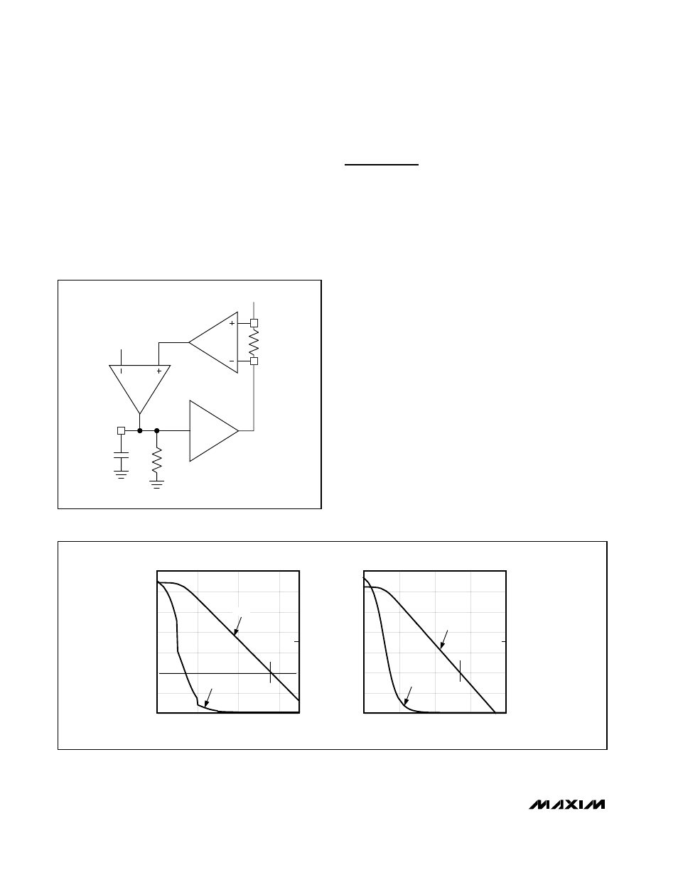
Figure 12. CCS Simplified Loop Diagram
CCI LOOP RESPONSE
MAGNITUDE (dB)
-90
-45
0
80
60
40
20
-40
-20
0
100
1k
10
0.1
100k
FREQUENCY (Hz)
CCS LOOP RESPONSE
MAGNITUDE (dB)
-90
-45
0
80
60
40
20
-40
-20
0
100
1k
10
0.1
100k
10M
FREQUENCY (Hz)
PHASE
PHASE
MAG
MAG
Figure 13. CCI and CCS Loop Response