Max1870a step-up/step-down li+ battery charger – Rainbow Electronics MAX1870A User Manual
Page 25
MAX1870A
Step-Up/Step-Down
Li+ Battery Charger
______________________________________________________________________________________
25
loop (CCS) is in control. Since the output capacitor’s
impedance has little effect on the response of the current
loop, only a single pole is required to compensate this
loop. A
CSI
and A
CSS
are the internal gains of the current-
sense amplifiers. RS2 is the charge current-sense resis-
tor. RS1a and RS1b are the adapter current-sense
resistors. R
OGMI
and R
OGMS
are the equivalent output
impedance of the GMI and GMS amplifiers, which are
greater than 10MΩ. GMI is the charge-current amplifier
transconductance (2.4µA/mV). GMS is the adapter-cur-
rent amplifier transconductance (1.7µA/mV.) GM
PWM
is
the DC-DC converter transconductance (1.85A/V).
Use the following equation to calculate the loop transfer
function:
which describes a single-pole system. Since GM
PWM
=
the loop-transfer function simplifies to:
Use the following equations to calculate the crossover
frequency:
For stability, choose a crossover frequency lower than
1/10th of the switching frequency and lower than half of
the RHP zero.
C
CI
= 10 GMI / (2π x f
OSC
), C
CS
= 10 GMS / (2π x f
OSC
)
This zero is inversely proportional to charge current
and may cause the system to go unstable at high cur-
rents when in step-up mode. A right-half-plane zero is
detrimental to both phase and gain. To also ensure sta-
bility under maximum load in step-up mode, the CCI
crossover frequency must also be lower than f
RHPZ
.
The right-half-plane zero does not affect CCS.
Choosing a crossover frequency of 30kHz and using
the component values listed in Figure 1 yields C
CI
and
C
CS_
> 10nF. Values for C
CI
/ C
CS
greater than ten
times the minimum value may slow down the current
loop response excessively. Figure 13 shows the Bode
Plot of the input-current frequency response using the
values calculated above.
MOSFET Drivers
DHI and DBST are optimized for driving moderately-
sized power MOSFETs. Use low-inductance and low-
resistance traces from driver outputs to MOSFET gates.
DHI typically sources 1.6A and sinks 0.8A to or from
the gate of the p-channel MOSFET. DHI swings from
VHP to VHN. VHN is a negative LDO that regulates with
respect to VHP to provide high-side gate drive.
Connect VHP to DCIN. Bypass VHN with a 1µF capaci-
tor to VHP.
f
V
x L I
V
L I
V
RHPZ WorstCase
IN MIN
L
IN MIN
OUTMAX
OUTMAX
_
_
_
=
=
2
2
2
π
π
f
GMI
C
f
GMS
C
CO CI
CI
CO CS
CS
_
_
,
=
=
2
2
π
π
LTF
GM
R
sR
x C
OGM
OGM
C
=
+
_
_
_
_
1
1
A
x RS
CS _
_
LTF
GM
x A
x RS
x GM
R
sR
x C
PWM
CS
OGM
OGM
C
=
+
_
_
_
_
_
_
1
CCV LOOP RESPONSE
MAGNITUDE (dB)
-135
-90
-45
0
80
60
40
20
-40
-20
0
1.E+00 1.E+01 1.E+02 1.E+03 1.E+04 1.E+05 1.E+06
1.E-01
FREQUENCY (Hz)
MAG
PHASE
Figure 10. CCV Loop Response
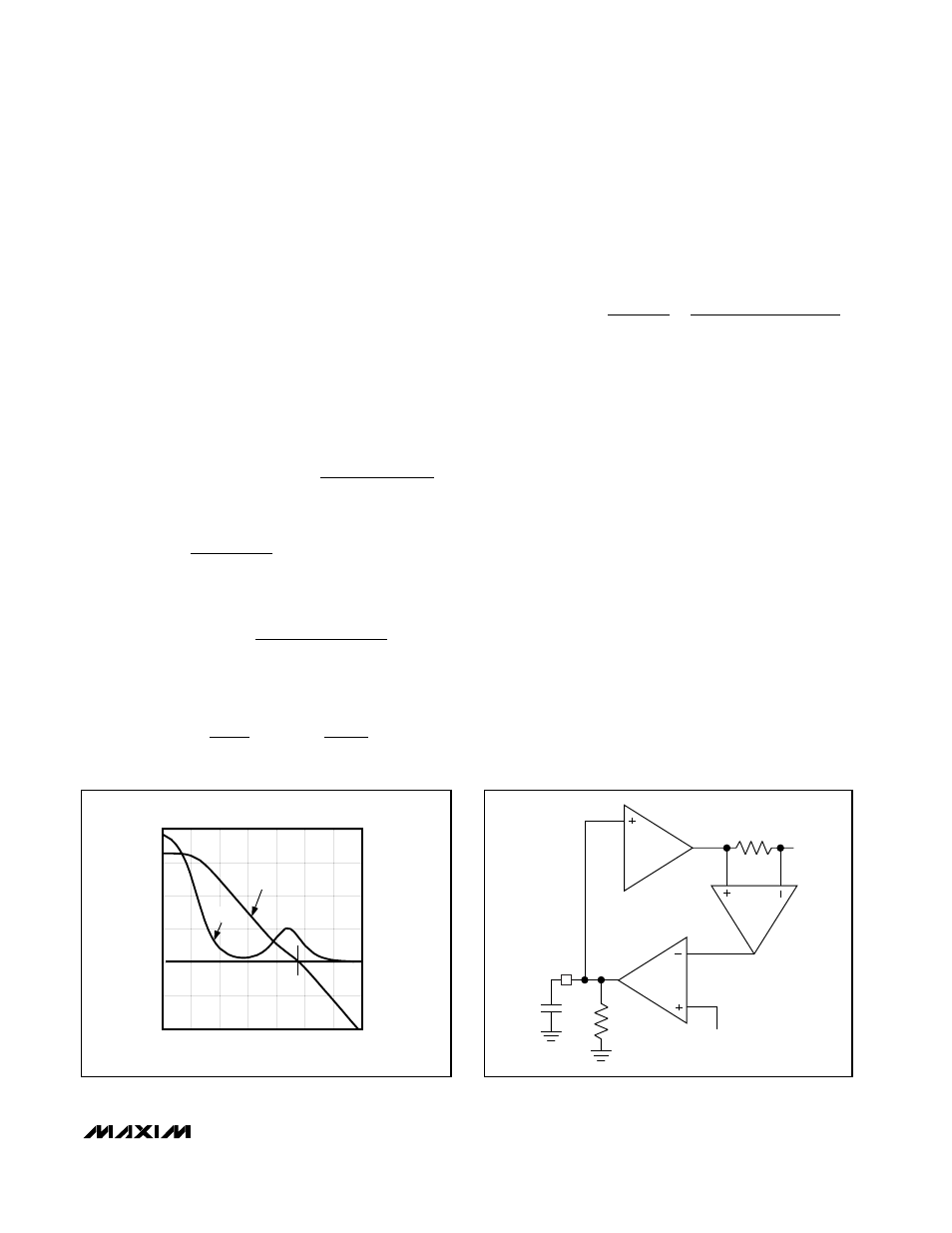
GM
PWM
REF
GMI
R
OGMI
C
CI
CCI
RS2
A
CSI
CSI
Figure 11. CCI Simplified Loop Diagram