Absolute maximum ratings, Operating ratings, Converter electrical characteristics – Rainbow Electronics ADC1175-50 User Manual
Page 5
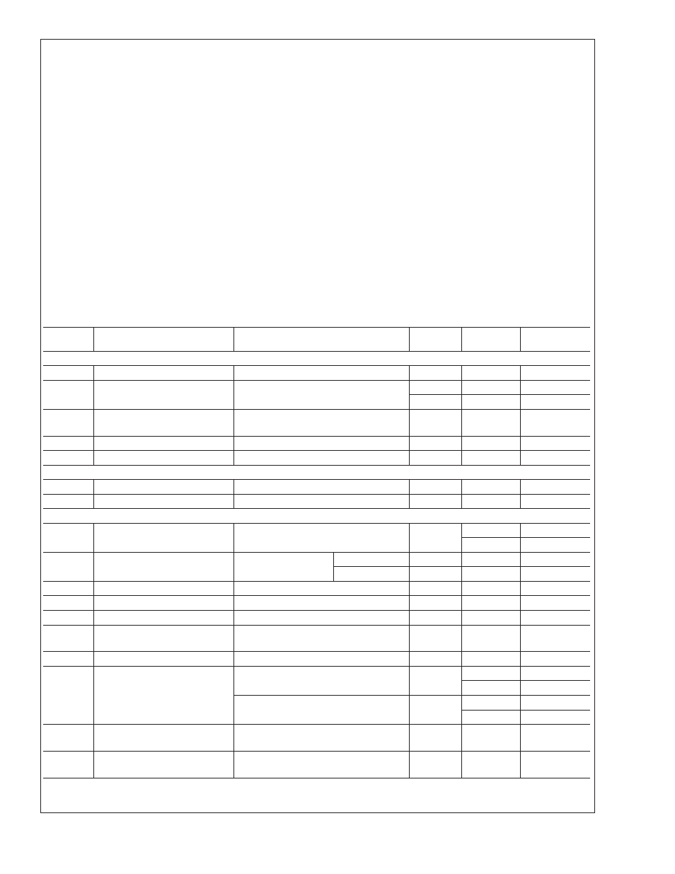
Absolute Maximum Ratings
(Notes 1, 2)
If Military/Aerospace specified devices are required,
please contact the National Semiconductor Sales Office/
Distributors for availability and specifications.
Supply Voltage (AV
DD
, DV
DD
)
6.5V
Voltage on Any Input or Output Pin
−0.3V to +6.5V
Reference Voltage (V
RT
, V
RB
)
AV
DD
to V
SS
CLK, PD Voltage Range
−0.5 to (AV
DD
+0.5V)
Digital Output Voltage (V
OH
, V
OL
)
V
DD
to V
SS
Input Current at Any Pin (Note 3)
±
25 mA
Package Input Current (Note 3)
±
50 mA
Power Dissipation at T
A
= 25˚C
See (Note 4)
ESD Susceptibility (Note 5)
Human Body Model
2000V
Machine Model
250V
Soldering Temperature, Infrared,
(10 sec.) (Note 6)
235˚C
Storage Temperature
−65˚C to +150˚C
Short Circuit Duration
(Single High Output to Ground)
1 Second
Operating Ratings
(Notes 1, 2)
Operating Temperature Range
−20˚C
≤
T
A
≤
+75˚C
Supply Voltage (AV
DD
, DV
DD
)
+4.75V to +5.25V
AV
DD
− DV
DD
<
0.5V
Ground Difference |DV
SS
–AV
SS
|
0V to 100 mV
Upper Reference Voltage (V
RT
)
1.0V to V
DD
Lower Reference Voltage (V
RB
)
0V to 4.0V
V
IN
Voltage Range
V
RB
to V
RT
Converter Electrical Characteristics
The following specifications apply for AV
DD
= DV
DD
= +5.0 V
DC
, PD = 0V, V
RT
= +2.6V, V
RB
= 0.6V, C
L
= 20 pF, f
CLK
=
50 MHz at 50% duty cycle. Boldface limits apply for T
A
= T
MIN
to T
MAX
; all other limits T
A
= 25˚C (Notes 7, 8).
Symbol
Parameter
Conditions
Typical
(Note 9)
Limits
(Note 9)
Units
(Limits)
DC ACCURACY
INL
Integral Non Linearity Error
V
IN
= 0.6V to 2.6V
±
0.8
±
1.95
LSB (max)
DNL
Differential Non-Linearity
V
IN
= 0.6V to 2.6V
+0.7
+1.75
LSB (max)
−0.7
−1.0
LSB (min)
Resolution for No Missing
Codes
8
Bits
E
OT
Top Offset Voltage
−12
mV
E
OB
Bottom Offset Voltage
+10
mV
VIDEO ACCURACY
DP
Differential Phase Error
f
IN
= 4.43 MHz Modulated Ramp
0.5
deg
DG
Differential Gain Error
f
IN
= 4.43 MHz Modulated Ramp
1.0
%
ANALOG INPUT AND REFERENCE CHARACTERISTICS
V
IN
Input Range
2.0
V
RB
V (min)
V
RT
V (max)
C
IN
V
IN
Input Capacitance
V
IN
= 1.5V
+0.7 Vrms
(CLK LOW)
4
pF
(CLK HIGH)
7
pF
R
IN
R
IN
Input Resistance
>
1
M
Ω
BW
Full Power Bandwidth
120
MHz
R
RT
Top Reference Resistor
320
Ω
R
REF
Reference Ladder Resistance
V
RT
to V
RB
270
200
350
Ω
(min)
Ω
(max)
R
RB
Bottom Reference Resistor
80
Ω
I
REF
Reference Ladder Current
V
RT
= V
RTS
, V
RB
= V
RBS
7
5.4
mA (min)
10.8
mA (max)
V
RT
= V
RTS
, V
RB
= AV
SS
8
6.1
mA (min)
12.3
mA (max)
V
RT
Reference Top Self Bias
Voltage
V
RT
Connected to V
RTS
, V
RB
Connected to V
RBS
2.6
V (min)
V (max)
V
RB
Reference Bottom Self Bias
Voltage
V
RT
Connected to V
RTS
, V
RB
Connected to V
RBS
0.6
0.55
0.70
V (min)
V (max)
ADC1
175-50
www.national.com
5