Applications information – Rainbow Electronics ADC1175-50 User Manual
Page 13
Applications Information
(All Schematic pin numbers refer to the TSSOP.) (Continued)
3.0 OUTPUT DATA TIMING
The Output Delay (t
OD
) of the ADC1175-50 can be very close
to one half clock cycle. Because of this, the output data
transition occurs very near the falling edge of the ADC clock.
To avoid clocking errors, you should use the
rising edge of
the ADC clock to latch the output data of the ADC1175-50
and
not use the falling edge.
4.0 POWER SUPPLY CONSIDERATIONS
Many A/D converters draw sufficient transient current to
corrupt their own power supplies if not adequately bypassed.
A 10 µF tantalum or aluminum electrolytic capacitor should
be placed within an inch (2.5 centimeters) of the A/D power
pins, with a 0.1 µF ceramic chip capacitor placed as close as
possible to the converter’s power supply pins. Leadless chip
capacitors are preferred because they have low lead induc-
tance.
While a single voltage source should be used for the analog
and digital supplies of the ADC1175-50, these supply pins
should be isolated from each other to prevent any digital
noise from being coupled to the analog power pins. We
recommended a choke be used between the analog and
digital supply lines, with a ceramic capacitor close to the
analog supply pin. If a resistor is used in place of the choke,
a maximum of 10
Ω
should be used.
The converter digital supply should
not be the supply that is
used for other digital circuitry on the board. It should be the
same supply used for the A/D analog supply.
As with all high speed converters, the ADC1175-50 should
be assumed to have little a.c. power supply rejection, espe-
cially when self biasing is used by connecting V
RT
and V
RTS
together.
No pin should ever have a voltage on it that is in excess of
the supply voltage or below ground, not even on a transient
basis. This can be a problem upon application of power to a
circuit. Be sure that the supplies to circuits driving the CLK,
PD, analog input and reference pins do not come up any
faster than does the voltage at the ADC1175-50 power pins.
5.0 THE ADC1175-50 CLOCK
Although the ADC1175-50 is tested and its performance is
guaranteed with a 50 MHz clock, it typically will function with
clock frequencies from 1 MHz to 55 MHz.
The clock should be one of low jitter and close to 50% duty
cycle.
6.0 LAYOUT AND GROUNDING
Proper grounding and proper routing of all signals is essen-
tial to ensure accurate conversion. Separate analog and
digital ground planes that are connected beneath the
ADC1175-50 are required to meet data sheet limits. The
analog and digital grounds may be in the same layer, but
should be separated from each other and should
never
overlap each other.
Capacitive coupling between the typically noisy digital
ground plane and the sensitive analog circuitry can lead to
poor performance that may seem impossible to isolate and
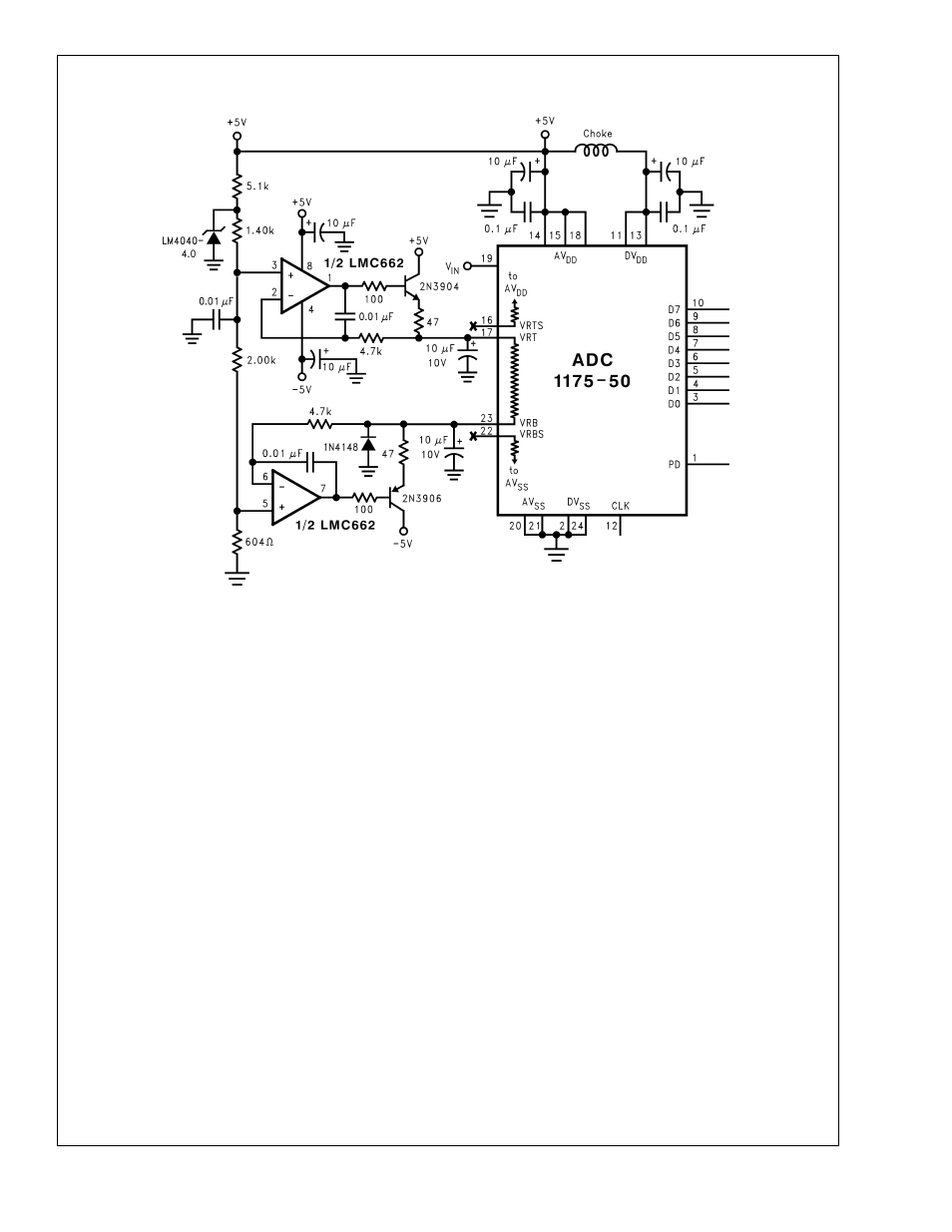
DS100896-27
FIGURE 5. Driving the Reference to Force Desired Values requires driving with a low impedance source, provided by
the transistors. Note that pins 16 and 22 are not connected.
ADC1
175-50
www.national.com
13