Timing diagram functional description – Rainbow Electronics ADC1175-50 User Manual
Page 10
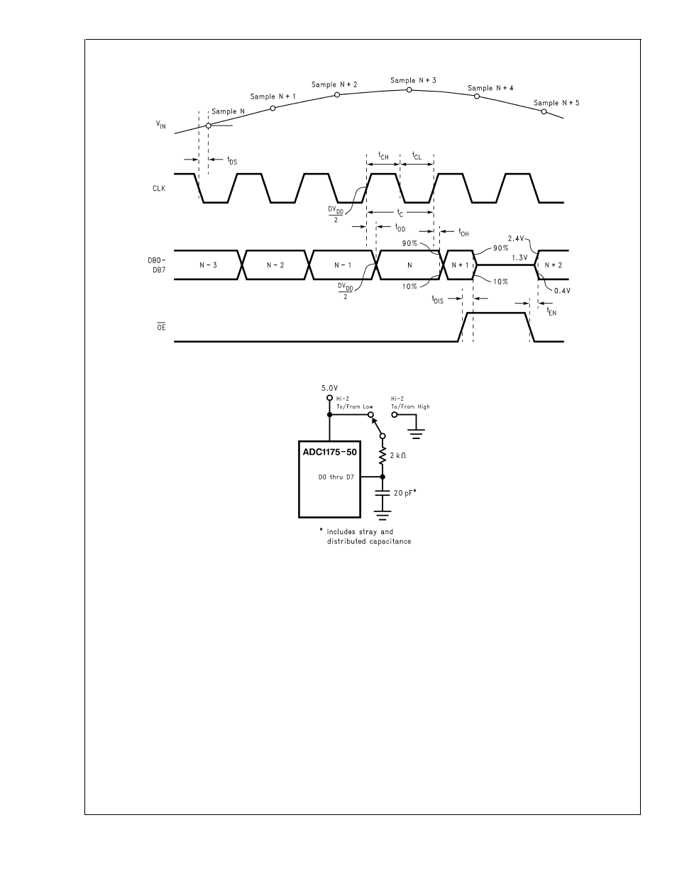
Timing Diagram
Functional Description
The ADC1175-50 maintains superior dynamic performance
with input frequencies up to 1/2 the clock frequency, achiev-
ing 6.8 effective bits with a 50 MHz sampling rate and
25 MHz input frequency.
The analog signal at V
IN
that is within the voltage range set
by V
RT
and V
RB
are digitized to eight bits at up to 55 MSPS.
Input voltages below V
RB
will cause the output word to
consist of all zeroes. Input voltages above V
RT
will cause the
output word to consist of all ones. While the ADC1175-50 is
optimized for top and bottom reference voltages (V
RT
and
V
RB
) or 2.6V and 0.6V, respectively, and will give best per-
formance at these values, V
RT
has a range of 1.0V to the
analog supply voltage, AV
DD
, while V
RB
has a range of 0V to
4.0V. V
RT
should always be at least 1.0V more positive than
V
RB
. With V
RT
voltages above 2.8V, it is necessary to reduce
the clock frequency to maintain SINAD performance.
If V
RT
and V
RTS
are connected together and V
RB
and V
RBS
are connected together, the nominal values of V
RT
and V
RB
are 2.6V and 0.6V, respectively. If V
RT
and V
RTS
are con-
nected together and V
RB
is grounded, the nominal value of
V
RT
is 2.3V.
Data is acquired at the falling edge of the clock and the
digital equivalent of that data is available at the digital out-
puts 2.5 clock cycles plus t
OD
later. The ADC1175-50 will
convert as long as the clock signal is present at the CLK pin.
The Power Down pin (PD), when high, puts the ADC1175-50
into a power down mode where power consumption is typi-
cally less than 5 mW. When the part is powered down, the
digital output pins are in a high impedance TRI-STATE. It
takes about 140 ns for the part to become active upon
coming out of the power down mode.
DS100896-23
FIGURE 1. ADC1175-50 Timing Diagram
DS100896-24
FIGURE 2. t
EN
, t
DIS
Test Circuit
ADC1
175-50
www.national.com
10