Applications information – Rainbow Electronics ADC1175-50 User Manual
Page 11
Applications Information
(All Schematic
pin numbers refer to the TSSOP.)
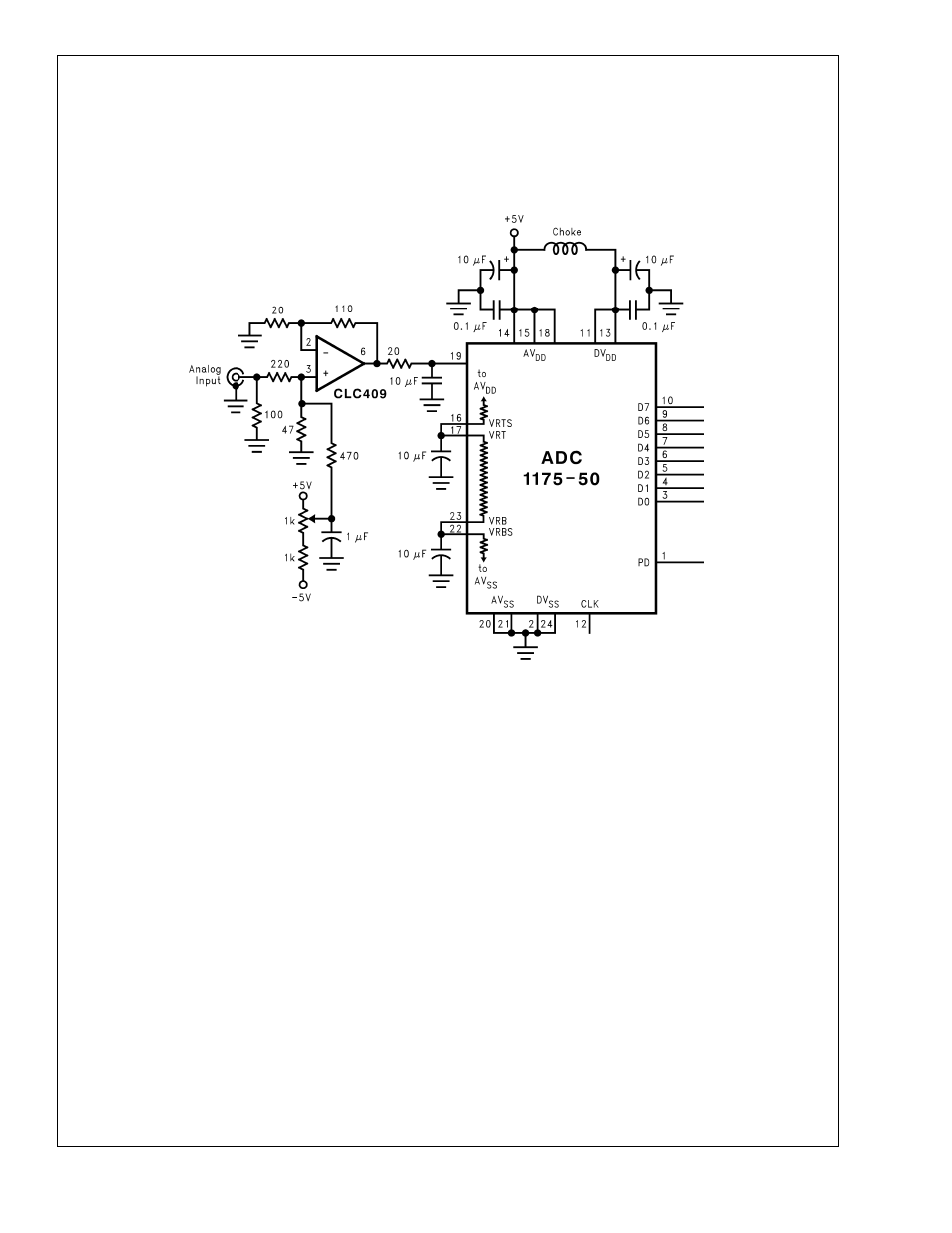
1.0 THE ANALOG INPUT
The analog input of the ADC1175-50 is a switch followed by
an integrator. The capacitance seen at the input changes
with the clock level, appearing as 4 pF when the clock is low,
and 7 pF when the clock is high. Since a dynamic capaci-
tance is more difficult to drive than is a fixed capacitance,
choose an amplifier that can drive this type of load. The
CLC409 has been found to be an excellent device for driving
the ADC1175-50. Do not drive the input beyond the supply
rails.
Figure 3 gives an example of driving circuitry.
2.0 REFERENCE INPUTS
The reference inputs V
RT
(Reference Top) and V
RB
(Refer-
ence Bottom) are the top and bottom of the reference ladder.
Input signals between these two voltages will be digitized to
8 bits. External voltages applied to the reference input pins
should be within the range specified in the Electrical Char-
acteristics table (1.0V to AV
DD
for V
RT
and 0V to (AV
DD
−
1.0V) for V
RB
). Any device used to drive the reference pins
should be able to source sufficient current into the V
RT
pin
and sink sufficient current from the V
RB
pin.
The reference ladder can be self-biased by connecting V
RT
to V
RTS
and connecting the V
RB
to V
RBS
to provide top and
bottom reference voltages of approximately 2.6V and 0.6V,
respectively, with V
CC
= 5.0V. This connection is shown in
Figure 3. If V
RT
and V
RTS
are tied together, but V
RB
is tied to
analog ground, a top reference voltage of approximately
2.3V is generated. The top and bottom of the ladder should
be bypassed with 10 µF tantalum capacitors located close to
the reference pins.
The reference self-bias circuit of
Figure 3 is very simple and
the performance is adequate for many applications. Better
linearity performance can generally be achieved by driving
the reference pins with a low impedance source.
By forcing a little current into or out of the top and bottom of
the ladder, as shown in
Figure 4, the top and bottom refer-
ence voltages can be trimmed and performance improved
over the self-bias method of
Figure 3. The resistive divider at
the amplifier inputs can be replaced with potentiometers, if
desired. The LMC662 amplifier shown was chosen for its low
offset voltage and low cost. Note that a negative power
supply is needed for these amplifiers as the lower one may
be required to go slightly negative to force the required
reference voltage.
If reference voltages are desired that are more than a few
tens of millivolts from the self-bias values, the circuit of
Figure 5 will allow forcing the reference voltages to whatever
levels are desired. This circuit provides the best performance
because of the low source impedance of the transistors.
Note that the V
RTS
and V
RBS
pins are left floating.
To minimize noise effects and ensure accurate conversions,
the total reference voltage range (V
RT
− V
RB
) should be a
minimum of 1.0V and a maximum of about 2.8V.
The ADC1175-50 is designed to operate with top and bottom
references of 2.6V and 0.6V, respectively. However, it will
function with reduced performance with a top reference volt-
age as high as AV
DD
.
DS100896-25
FIGURE 3. Driving the ADC1175-50. Choose an op-amp that can drive a dynamic capacitance.
ADC1
175-50
www.national.com
11