Ata6832, Absolute maximum ratings, Thermal resistance – Rainbow Electronics ATA6832 User Manual
Page 8: Operating range
8
4951A–AUTO–08/06
ATA6832
4.
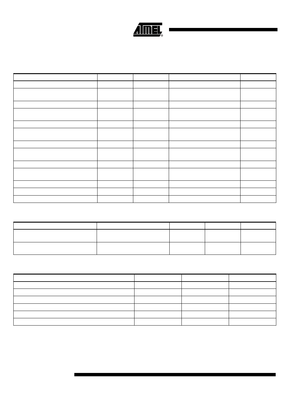
Absolute Maximum Ratings
Stresses beyond those listed under “Absolute Maximum Ratings” may cause permanent damage to the device. This is a stress rating
only and functional operation of the device at these or any other conditions beyond those indicated in the operational sections of this
specification is not implied. Exposure to absolute maximum rating conditions for extended periods may affect device reliability.
Parameters
Pin
Symbol
Value
Unit
Supply voltage
10, 11
V
VS
–0.3 to +40
V
Supply voltage
t < 0.5s; I
S
> –2A
10, 11
V
VS
–1
V
Logic supply voltage
9
V
VCC
–0.3 to +7
V
Logic input voltage
3, 4, 5, 6
V
CS
, V
DI
, V
CLK
,
V
PWM
–0.3 to V
VCC
+ 0.3
V
Logic output voltage
7
V
DO
–0.3 to V
VCC
+ 0.3
V
Input current
3, 4, 5, 6
I
CS
, I
DI
, I
CLK
,
I
PWM
–10 to +10
mA
Output current
7
I
DO
–10 to +10
mA
Output current
2, 12, 15
I
Out1
, I
Out2
, I
Out3
Internally limited, see output
specification
Output voltage
2, 12, 15
I
Out1
, I
Out2
, I
Out3
–0.3 to +40
V
Reverse conducting current
(t
pulse
= 150 µs)
2, 12, 15
I
Out1
, I
Out2
, I
Out3
17
A
Junction temperature range
T
j
–40 to +150
°C
Storage temperature range
T
STG
–55 to +150
°C
Ambient temperature range
T
a
–40 to +150
°C
5.
Thermal Resistance
Parameters
Test Conditions
Symbol
Value
Unit
Thermal resistance from junction to
case
R
thJC
15
k/W
Thermal resistance from junction to
ambient
Depends on the PC board
R
thJA
40
K/W
6.
Operating Range
Parameters
Symbol
Value
Unit
Supply voltage
V
VS
V
UV
(1)
to 40
V
Logic supply voltage
V
VCC
4.75 to 5.25
V
Logic input voltage
V
CS
, V
DI
, V
CLK
,
V
PWM
–0.3 to V
VCC
V
Serial interface clock frequency
f
CLK
2
MHz
PWM input frequency
f
PWM
max. 25
kHz
Junction temperature range
T
j
–40 to +150
°C
Note:
1. Threshold for undervoltage description