Rainbow Electronics DS12887 User Manual
Page 4
DS12887
4 of 19
SIGNAL DESCRIPTIONS
GND, V
CC
– DC power is provided to the device on these pins. V
CC
is the +5V input. When 5V are
applied within normal limits, the device is fully accessible and data can be written and read. When V
CC
is
below 4.25V typical, reads and writes are inhibited. However, the timekeeping function continues
unaffected by the lower input voltage. As V
CC
falls below 3V typical, the RAM and timekeeper are
switched over to an internal lithium energy source. The timekeeping function maintains an accuracy of
±1
minute per month at +25
°C, regardless of the voltage input on the V
CC
pin.
MOT (Mode Select) – The MOT pin offers the flexibility to choose between two bus types. When
connected to V
CC
, Motorola bus timing is selected. When connected to GND or left disconnected, Intel
bus timing is selected. The pin has an internal pulldown resistance of approximately 20k
W.
SQW (Square-Wave Output) – The SQW pin can output a signal from one of 13 taps provided by the
15 internal divider stages of the RTC. The frequency of the SQW pin can be changed by programming
Register A, as shown in Table 1. The SQW signal can be turned on and off using the SQWE bit in
Register B. The SQW signal is not available when V
CC
is less than 4.25V, typically.
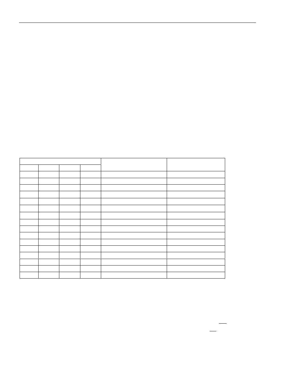
Table 1
.
PERIODIC INTERRUPT RATE AND SQUARE-WAVE OUTPUT
FREQUENCY
SELECT BITS REGISTER A
RS3
RS2
RS1
RS0
t
PI
PERIODIC
INTERRUPT RATE
SQW OUTPUT
FREQUENCY
0
0
0
0
None
None
0
0
0
1
3.90625ms
256Hz
0
0
1
0
7.8125ms
128Hz
0
0
1
1
122.070
ms
8.192kHz
0
1
0
0
244.141
ms
4.096kHz
0
1
0
1
488.281
ms
2.048kHz
0
1
1
0
976.5625
ms
1.024kHz
0
1
1
1
1.953125ms
512Hz
1
0
0
0
3.90625ms
256Hz
1
0
0
1
7.8125ms
128Hz
1
0
1
0
15.625ms
64Hz
1
0
1
1
31.25ms
32Hz
1
1
0
0
62.5ms
16Hz
1
1
0
1
125ms
8Hz
1
1
1
0
250ms
4Hz
1
1
1
1
500ms
2Hz
AD0–AD7 (Multiplexed Bidirectional Address/Data Bus) – Multiplexed buses save pins because
address information and data information time-share the same signal paths. The addresses are present
during the first portion of the bus cycle and the same pins and signal paths are used for data in the second
portion of the cycle. Address/data multiplexing does not slow the access time of the DS12887 since the
bus change from address to data occurs during the internal RAM access time. Addresses must be valid
prior to the falling edge of AS/ ALE, at which time the DS12887 latches the address from AD0 to AD6.
Valid write data must be present and held stable during the latter portion of the DS or
WR
pulses. In a
read cycle the DS12887 outputs 8 bits of data during the latter portion of the DS or
RD
pulses. The read