Rainbow Electronics ATF2500CQL User Manual
Features, Block diagram description, Pin configurations
1
Features
•
High-performance, High-density, Electrically-erasable Programmable Logic Device
•
Fully Connected Logic Array with 416 Product Terms
•
10 ns Maximum Pin-to-pin Delay for 5V Operation
•
Low-power Edge-sensing “L” Option with <1 mA Standby Current
•
24 Flexible Output Macrocells
– 48 Flip-flops – Two per Macrocell
– 72 Sum Terms
– All Flip-flops, I/O Pins Feed in Independently
•
D- or T-type Flip-flops
•
Product Term or Direct Input Pin Clocking
•
Registered or Combinatorial Internal Feedback
•
Backward Compatible with ATV2500B/BQL and ATV2500H/L Software
•
Advanced Electrically-erasable Technology
– Reprogrammable
– 100% Tested
•
44-lead Surface Mount Package
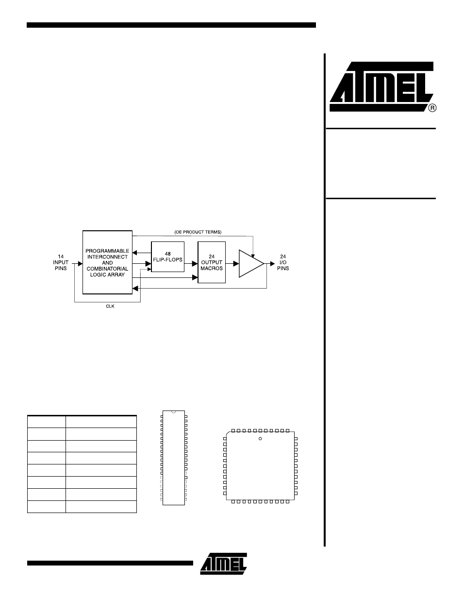
Block Diagram
Description
The ATF2500C is the highest-density PLD available in a 44-pin package. With its fully
connected logic array and flexible macrocell structure, high gate utilization is easily
obtainable. The ATF2500C is a high-performance CMOS (electrically-erasable) pro-
grammable logic device (PLD) that utilizes Atmel’s proven electrically-erasable
technology.
ATF2500C
CPLD Family
Datasheet
ATF2500C
ATF2500CL
ATF2500CQ
ATF2500CQL
Preliminary
Rev. 0777G–12/01
Pin Configurations
Pin Name
Function
IN
Logic Inputs
CLK/IN
Pin Clock and Input
I/O
Bi-directional Buffers
I/O 0,2,4...
“Even” I/O Buffers
I/O 1,3,5...
“Odd” I/O Buffers
GND
Ground
VCC
+5V Supply
DIP
1
2
3
4
5
6
7
8
9
10
11
12
13
14
15
16
17
18
19
20
40
39
38
37
36
35
34
33
32
31
30
29
28
27
26
25
24
23
22
21
IN
IN
IN
I/O0
I/O1
I/O2
I/O3
I/O4
I/O5
VCC
I/O17
I/O16
I/O15
I/O14
I/O13
I/O12
IN
IN
IN
IN
IN
IN
IN
IN
I/O6
I/O7
I/O8
I/O9
I/O10
I/O11
GND
I/O23
I/O22
I/O21
I/O20
I/O19
I/O18
IN
IN
IN
PLCC/LCC/JLCC
7
8
9
10
11
12
13
14
15
16
17
39
38
37
36
35
34
33
32
31
30
29
I/O2
I/O3
I/O4
I/O5
VCC
VCC
I/O17
I/O16
I/O15
I/O14
I/O13
I/O7
I/O8
I/O9
I/O10
I/O11
GND
GND
I/O23
I/O22
I/O21
I/O20
6
5
4
3
2
1
44
43
42
41
40
18
19
20
21
22
23
24
25
26
27
28
I/O12
IN
IN
IN
IN
IN
IN
IN
IN
I/O18
I/O19
I/O1
I/O0
GND
IN
IN
CLK/IN
IN
IN
IN
IN
I/O6
Note:
For ATF2500CQ and ATF2500CQL
(PLCC/LCC/JLCC packages) pin 4 and pin 26
GND connections are not required.
Document Outline
- Features
- Block Diagram
- Description
- Using the ATF2500C Family’s Many Advanced Features
- Power-up Reset
- Preload and Observability of Registered Outputs
- Programming Software Support
- Security Fuse Usage
- Input and I/O Pull-ups
- Input Diagram
- I/O Diagram
- Functional Logic Diagram Description
- Functional Logic Diagram ATV2500C
- Output Logic, Registered(1)
- Output Logic, Combinatiorial(1)
- Clock Option
- Absolute Maximum Ratings*
- DC and AC Operating Conditions
- Pin Capacitance
- Test Waveforms and Measurement Levels
- Output Test Load
- AC Waveforms(1) Input Pin Clock
- AC Waveforms(1) Product Term Clock
- AC Waveforms(1) Combinatorial Outputs and Feedback
- ATF2500C DC Characteristics
- ATF2500C AC Characteristics
- ATF2500C Register AC Characteristics, Input Pin Clock
- ATF2500C Register AC Characteristics, Product Term Clock
- ATF2500CL DC Characteristics
- ATF2500CL AC Characteristics
- ATF2500CL Register AC Characteristics, Input Pin Clock
- ATF2500CL Register AC Characteristics, Product Term Clock
- ATF2500CQ DC Characteristics
- ATF2500CQ Register AC Characteristics, Input Pin Clock
- ATF2500CQ Register AC Characteristics, Product Term Clock
- ATF2500CQL AC Characteristics
- ATF2500CQL Register AC Characteristics, Input Pin Clock
- ATF2500CQL Register AC Characteristics, Product Term Clock
- Ordering Information
- Using “C” Product for Industrial
- Packaging Information