Input diagram, I/o diagram, Speed/power management – Rainbow Electronics ATF1502ASV User Manual
Page 6: Atf1502asv, Input diagram i/o diagram speed/power management
6
ATF1502ASV
1615G–PLD–09/02
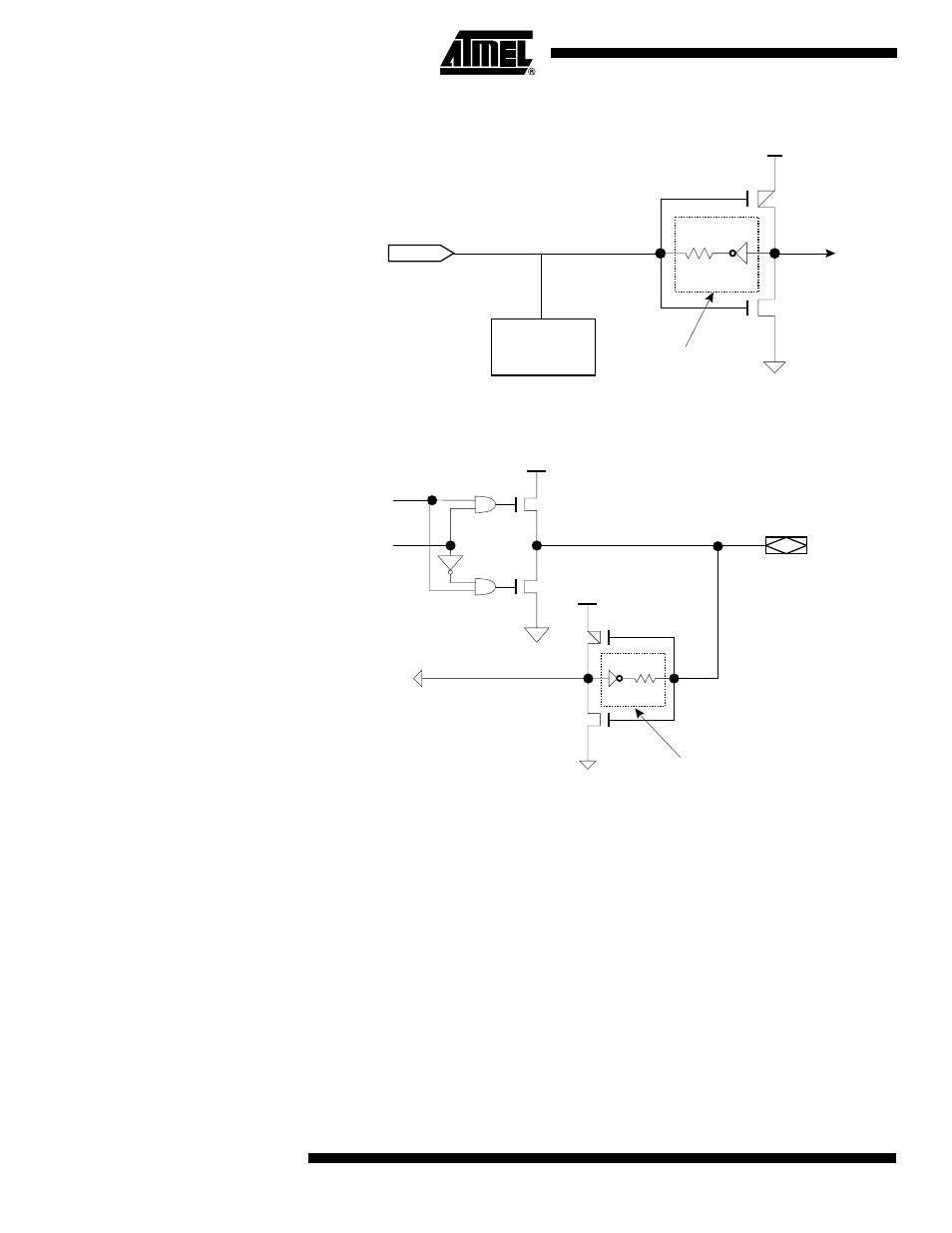
Input Diagram
I/O Diagram
Speed/Power
Management
The ATF1502ASV has several built-in speed and power management features.
To further reduce power, each ATF1502ASV macrocell has a reduced-power bit feature.
To reduce power consumption this feature may be actived (by changing the default
value of OFF to ON) for any or all macrocells.
The ATF1502ASV also has an optional power-down mode. In this mode, current drops
to below 15 mA. When the power-down option is selected, either PD1 or PD2 pins (or
both) can be used to power down the part. The power-down option is selected in the
design source file. When enabled, the device goes into power-down when either PD1 or
PD2 is high. In the power-down mode, all internal logic signals are latched and held, as
are any enabled outputs.
All pin transitions are ignored until the PD pin is brought low. When the power-down fea-
ture is enabled, the PD1 or PD2 pin cannot be used as a logic input or output. However,
the pin’s macrocell may still be used to generate buried foldback and cascade logic
signals.
V
CC
PROGRAMMABLE
OPTION
100K
INPUT
ESD
PROTECTION
CIRCUIT
OE
DATA
V
CC
PROGRAMMABLE
OPTION
100K
V
CC
I/O