Power-down mode, Power-down ac characteristics(1)(1), Absolute maximum ratings – Rainbow Electronics ATF1502ASV User Manual
Page 10: Atf1502asv, Power-down ac characteristi cs
10
ATF1502ASV
1615G–PLD–09/02
Power-down Mode
The ATF1502ASV includes an optional pin-controlled power-down feature. When this
mode is enabled, the PD pin acts as the power-down pin. When the PD pin is high, the
device supply current is reduced to less than 3 mA. During power-down, all output data
and internal logic states are latched and held. Therefore, all registered and combinato-
rial output data remain valid. Any outputs that were in a high-Z state at the onset will
remain at high-Z. During power-down, all input signals except the power-down pin are
blocked. Input and I/O hold latches remain active to ensure that pins do not float to inde-
terminate levels, further reducing system power. The power-down pin feature is enabled
in the logic design file. Designs using the power-down pin may not use the PD pin logic
array input. However, all other PD pin macrocell resources may still be used, including
the buried feedback and foldback product term array inputs.
Notes:
1. For slow slew outputs, add t
SSO
.
1. Pin or product term.
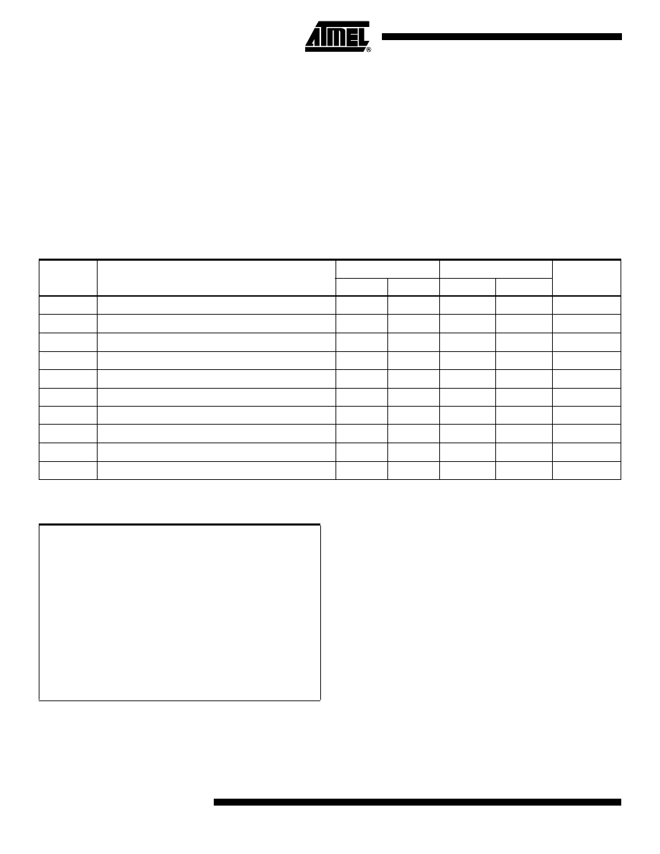
Power-down AC Characteristics
(1)(1)
Symbol
Parameter
-15
-20
Units
Min
Max
Min
Max
t
IVDH
Valid I, I/O before PD High
15
20
ns
t
GVDH
Valid OE
(1)
before PD High
15
20
ns
t
CVDH
Valid Clock
(1)
before PD High
15
20
ns
t
DHIX
I, I/O Don’t Care after PD High
25
30
ns
t
DHGX
OE
(1)
Don’t Care after PD High
25
30
ns
t
DHCX
Clock
(1)
Don’t Care after PD High
25
30
ns
t
DLIV
PD Low to Valid I, I/O
1
1
µs
t
DLGV
PD Low to Valid OE
(1)
1
1
µs
t
DLCV
PD Low to Valid Clock
(1)
1
1
µs
t
DLOV
PD Low to Valid Output
1
1
µs
Absolute Maximum Ratings*
Temperature Under Bias .................................. -40°C to +85°C
*NOTICE:
Stresses beyond those listed under “Absolute
Maximum Ratings” may cause permanent dam-
age to the device. This is a stress rating only and
functional operation of the device at these or any
other conditions beyond those indicated in the
operational sections of this specification is not
implied. Exposure to absolute maximum rating
conditions for extended periods may affect device
reliability.
Note:
1. Minimum voltage is -0.6V DC, which may under-
shoot to -2.0V for pulses of less than 20 ns.
Maximum output pin voltage is V
CC
+ 0.75V DC,
which may overshoot to 7.0V for pulses of less
than 20 ns.
Storage Temperature ..................................... -65°C to +150°C
Voltage on Any Pin with
Respect to Ground .........................................-2.0V to +7.0V
(1)
Voltage on Input Pins
with Respect to Ground
During Programming.....................................-2.0V to +14.0V
(1)
Programming Voltage with
Respect to Ground .......................................-2.0V to +14.0V
(1)